
Manual
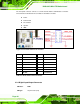
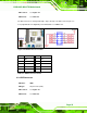
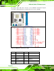
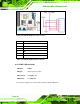
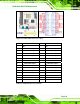
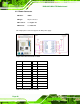

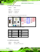
Table Of Contents
- 1 Introduction
- 2 Detailed Specifications
- 3 Unpacking
- 4 Connector Pinouts
- 4.1 Peripheral Interface Connectors
- 4.2 Internal Peripheral Connectors
- 4.2.1 Fan Connectors
- 4.2.2 Front Panel Connector
- 4.2.3 Digital Input/Output Connector
- 4.2.4 IDE Connector
- 4.2.5 LCD Backlight Connector
- 4.2.6 LVDS LCD connector
- 4.2.7 Power Connector
- 4.2.8 14-Pin Serial Port Connectors
- 4.2.9 10-Pin Serial Port Connectors
- 4.2.10 SATA Drive Connectors
- 4.2.11 SPDIF Connector
- 4.2.12 Internal USB Connectors
- 4.3 External Interface Connectors
- 5 Installation
- 6 AMI BIOS
- 7 Driver Installation
- A BIOS Options
- B DIO Interface
- C Watchdog Timer
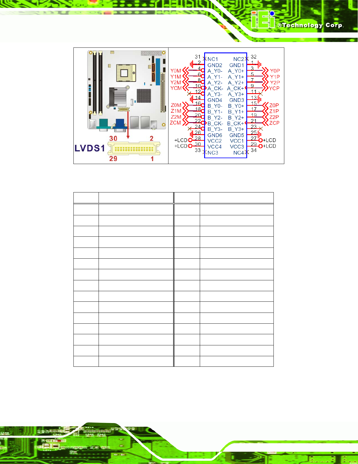
KINO-9453 Mini-ITX Motherboard
Page 39
Figure 4-7: LVDS LCD Connector Location
PIN NO. DESCRIPTION PIN NO. DESCRIPTION
1 GND 2 GND
3 1
st
LVDS data0 output + 4 1
st
LVDS data0 output -
5 1
st
LVDS data1 output + 6 1
st
LVDS data1 output -
7 1
st
LVDS data2 output + 8 1
st
LVDS data2 output -
9 1
st
LVDS clock output + 10 1
st
LVDS clock output -
11 NC 12 NC
13 GND 14 GND
15 2
nd
LVDS data0 output + 16 2
nd
LVDS data0 output -
17 2
nd
LVDS data1 output + 18 2
nd
LVDS data1 output -
19 2
nd
LVDS data2 output + 20 2
nd
LVDS data2 output -
21 2
nd
LVDS clock output + 22 2
nd
LVDS clock output -
23 NC 24 NC
25 GND 26 GND
27 +LCD (3.3V, 5V or 12V) 28 +LCD (3.3V, 5V or 12V)
29 +LCD (3.3V, 5V or 12V) 30 +LCD (3.3V, 5V or 12V)
Table 4-8: LVDS LCD Connector Pinouts