
Manual
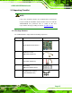
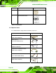
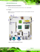
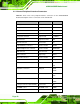
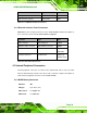
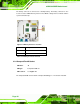
Table Of Contents
- 1 Introduction
- 2 Detailed Specifications
- 3 Unpacking
- 4 Connectors
- 4.1 Peripheral Interface Connectors
- 4.2 Internal Peripheral Connectors
- 4.2.1 BIOS Battery Connector
- 4.2.2 CompactFlash® Socket
- 4.2.3 Digital I/O Connector
- 4.2.4 Fan Connector
- 4.2.5 Front Panel Connector
- 4.2.6 IDE Connector
- 4.2.7 Infrared Interface Connector
- 4.2.8 Keyboard/Mouse Connector
- 4.2.9 LCD Backlight Inverter Connector
- 4.2.10 LED Connector
- 4.2.11 LVDS LCD Connector
- 4.2.12 MCU LAN Connector
- 4.2.13 PCIe Mini Card Slot
- 4.2.14 Power Connectors
- 4.2.15 SATA Drive Connectors
- 4.2.16 SATA Power Connectors
- 4.2.17 Serial Port Connectors (RS-232)
- 4.2.18 Serial Port Connectors (RS-422/485)
- 4.2.19 SO-DIMM Socket
- 4.2.20 SPDIF Connector
- 4.2.21 TV Out Connector
- 4.2.22 USB Connectors
- 4.3 External Peripheral Interface Connector Panel
- 5 Installation
- 6 BIOS Setup
- 7 Software Installation
- 8 Battery Monitoring
- A BIOS Options
- B Terminology
- C Digital I/O Interface
- D Watchdog Timer
- E Address Mapping
- F Hazardous Materials Disclosure
eKINO-945GSE Motherboard
Page 33
Connector Type Label
TV output connector 6-pin header TV1
USB connector (2 ports) 8-pin header USB1
Table 4-1: Peripheral Interface Connectors
4.1.3 External Interface Panel Connectors
8Table 4-2 lists the rear panel connectors on the eKINO-945GSE. Detailed descriptions of
these connectors can be found in Section 1H
4.3 on page 855.
Connector Type Label
Audio connector Dual audio jack AUDIO1
VGA/DVI combo connector VGA and DVI connector VIDEO1
LAN/USB combo connector LAN and 2 x USB LAN/USB1
LAN/USB2
Serial port connector 2 x DB-9 male COM1 (top)
COM2 (bottom)
Table 4-2: Rear Panel Connectors
4.2 Internal Peripheral Connectors
Internal peripheral connectors are found on the motherboard and are only accessible
when the motherboard is outside of the chassis. This section has complete descriptions of
all the internal, peripheral connectors on the eKINO-945GSE.
4.2.1 BIOS Battery Connector
CN Label: BT1
CN Type:
2-pin wafer (1x2)
CN Location:
See
Figure 4-2
CN Pinouts:
See
Table 4-3