
Owner's manual


Table Of Contents
- 42AFL-xxA-N270 Series Flat Panel PC
- 1 Introduction
- 2 Detailed Specifications
- 3 Unpacking
- 4 Installation
- 4.1 Anti-static Precautions
- 4.2 Installation Precautions
- 4.3 Preinstalled Components
- 4.4 Installation and Configuration Steps
- 4.5 Removing the Back Cover
- 4.6 CF Card Installation
- 4.7 HDD Installation (AF-12A-N270 Only)
- 4.8 AT/ATX Mode Selection
- 4.9 Jumper Settings
- 4.10 Mounting the System
- 4.11 Bottom Panel Connectors
- 5 System Maintenance
- 6 AMI BIOS Setup
- 7 Software Drivers
- A System Specifications
- B Safety Precautions
- C BIOS Configuration Options
- D Watchdog Timer
- E Hazardous Materials Disclosure
- F Index
AFL-xxA-N270 Series Panel PC
Page 38
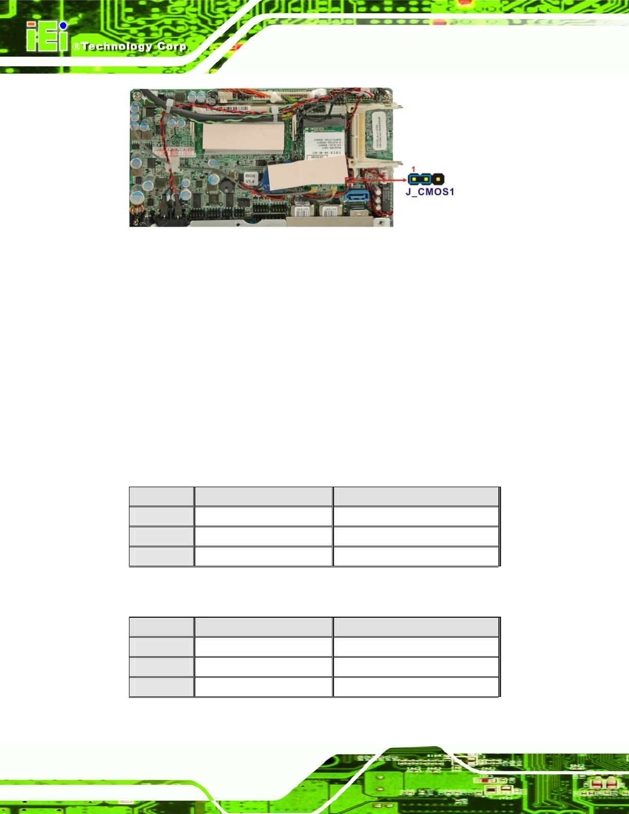
Figure 4-7: Clear CMOS Jumper
4.9.4 COM Port Pin 9 Select
Jumper Label:
JP8 and JP10
Jumper Settings:
See
Table 4-4
Jumper Location:
See
Figure 4-8
Two jumpers (JP8 and JP10) configure pin 9 on COM1 and COM3 DB-9 connectors. Pin 9
on the COM1 and the COM3 DB-9 connectors can be set as the ring (RI) signal, +5 V or
+12 V. The COM1 and COM3 Pin 9 Setting jumper selection options are shown in
Table
4-4.
JP8 Description
Short 1-3 COM1 RI Pin use +12 V
Short 5-7 COM1 RI Pin use +5 V
Short 7-9 COM1 RI Pin use RI Default
Table 4-4: COM1 Pin 9 Setting Jumper Settings
JP10 Description
Short 1-2 COM3 RI Pin use +12 V
Short 3-4 COM3 RI Pin use RI Default
Short 5-6 COM3 RI Pin use +5 V
Table 4-5: COM3 Pin 9 Setting Jumper Settings