
User Manual

AFL-F08A Panel PC
Page 22
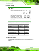
Clear CMOS Description
Short 1 - 2 Keep CMOS Setup Default
Short 2 - 3 Clear CMOS Setup
Table 3-3: Clear CMOS Jumper Settings
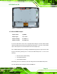
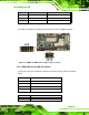
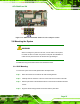
The location of the clear CMOS jumper is shown in Figure 3-8 below.
Figure 3-8: Clear CMOS Jumper
3.7.5 COM Port Pin 9 Select
Jumper Label:
JP8 and JP10
Jumper Settings:
See
Table 3-4
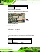
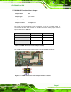
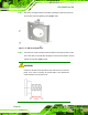
Jumper Location:
See
Figure 3-9
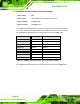
Two jumpers (JP8 and JP10) configure pin 9 on COM1 and COM3 DB-9 connectors. Pin 9
on the COM1 and the COM3 DB-9 connectors can be set as the ring (RI) signal, +5 V or
+12 V. The COM1 and COM3 Pin 9 Setting jumper selection options are shown in
Table
3-4.
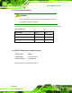
JP8 Description
Short 1-3 COM1 RI Pin use +12 V
Short 5-7 COM1 RI Pin use +5 V
Short 7-9 COM1 RI Pin use RI Default
Table 3-4: COM1 Pin 9 Setting Jumper Settings