
User Manual
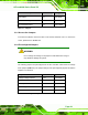


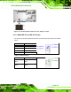


Table Of Contents
- 1 Introduction
- 2 Unpacking
- 3 Installation
- 4 System Maintenance
- 5 AMI BIOS Setup
- 5.1 Introduction
- 5.2 Main
- 5.3 Advanced
- 5.4 iEi Feature
- 5.5 Chipset
- 5.6 Boot
- 5.7 Security
- 5.8 Save & Exit
- 6 Software Drivers
- 7 Interface Connectors
- 7.1 Peripheral Interface Connectors
- 7.2 Internal Peripheral Connectors
- 7.2.1 Audio Speaker-out Connector (CN3)
- 7.2.2 Audio MIC-in Connector (MIC1)
- 7.2.3 Audio DMIC-in Connector (DMIC1)
- 7.2.4 Battery Connector (CN1)
- 7.2.5 COM2 Connector (COM2)
- 7.2.6 CPU Fan Connector (CPU_FAN1)
- 7.2.7 DIO Connector (DIO1)
- 7.2.8 HDD LED Connector (HDD_CN1)
- 7.2.9 I2C Connector (CN4)
- 7.2.10 LVDS Connector (LVDS1)
- 7.2.11 LVDS Backlight Connector (INVERTER1)
- 7.2.12 MCU Connector (JP8)
- 7.2.13 MCU Connector (HOTKEY_CN1)
- 7.2.14 PCIe Mini Slot (M_PCIE1)
- 7.2.15 PCIe Mini Slot (M_PCIE2)
- 7.2.16 Power LED Connector (PW_LED1)
- 7.2.17 Power Button Connector (PW_BTN1)
- 7.2.18 SATA Power Connector (SATA_PWR1)
- 7.2.19 SATA Connector (SATA1)
- 7.2.20 Touch Panel Connector (TS1)
- 7.2.21 TTL Panel Connector (CN6)
- 7.2.22 USB Connector (USB1)
- 7.2.23 USB Connector (USB2)
- 7.2.24 USB Connector (USB3)
- 7.2.25 USB2 and USB3 Power Connector (JP18)
- 7.3 External Interface Panel Connectors
- 7.4 Preconfigured Jumper Settings
- A Safety Precautions
- B BIOS Configuration Options
- C Watchdog Timer
- D Hazardous Materials Disclosure
AFL-xxA-N26 Series Panel PC
Page 45
Figure 3-13: Clear CMOS Jumper
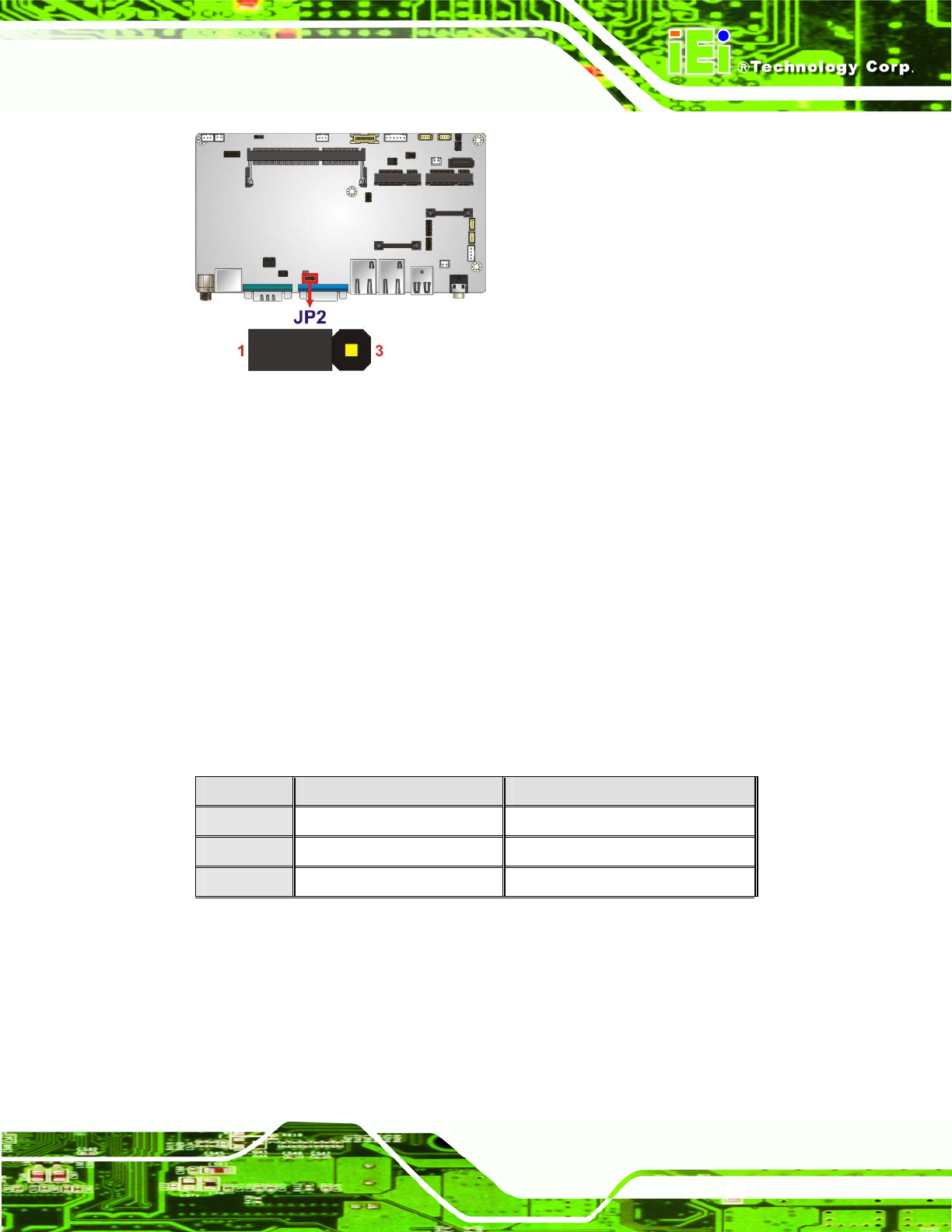
3.8.4 COM3 Port Pin 9 Select
Jumper Label:
JP5
Jumper Type:
6-pin header
Jumper Settings:
See
Table 3-4
Jumper Location:
See
Figure 3-14
This jumper configures pin 9 on COM3 DB-9 connector. Pin 9 on the COM3 DB-9
connector can be set as the ring (RI) signal, +5 V or +12 V. The COM3 Pin 9 Setting
jumper selection options are shown in
Table 3-4.
JP5 Description
Short 1-2 COM1 RI Pin use +12 V
Short 3-4 COM1 RI Pin use RI Default
Short 5-6 COM1 RI Pin use +5 V
Table 3-4: COM3 Pin 9 Setting Jumper Settings
The COM3 Pin 9 Setting jumper location is shown in Figure 3-14 below.