
User Manual

1.7 Reconfiguring the 7521(D)/7522(D)/7523(D)
From pin-4 to pin-8 of the 7521/7522/7523 there are three D/O & two D/I
pins. For the application of “Customized 7000 Modules”, these 5 D/I/O pins
can be hardware reconfigured to other functions as follows:
Step 1: Remove the reconfiguration-resistor as follows:
If DO3 is reconfigured, remove R19
If DO2 is reconfigured, remove R20
If DO1 is reconfigured, remove R21
If DI3 is reconfigured, remove R22
If DI2 is reconfigured, remove R23
Then, the onboard D/I/O functions can be disabled.
Step 2: Install a 5-pin male reconfiguration-jumper into the TP0 of the
7521(D)/7522(D)/7523(D)
Step 3: Design a 5-pin female reconfiguration-jumper in X??? for
connection to TP1. Then the external signals from pin-4 to pin-8
can be connected to X???. The user can refigure these 5 D/I/O pins
to their special requirements now.
Note: If the DO2 is reconfigured to D/I, its initial state must be High. If its
initial state is LOW, system clock will be reduced to 10M. So all
clock-related libraries will only be at half-speed.
The X100 is an 8-channel D/I board designed for the 7521/7522/7523. It
removes all 5 resistors, R19 ~ R23, and reconfigures all these pins as D/I pins.
It installs another 5-pin female reconfiguration-jumper into TP1 of the
7521/7522/7523.
Therefore, user can select the original 3_DO_2_DI functions or new
5_DI functions by setting the jumper in different positions. Refer to “I/O
Expansion Bus in the 7188X/7188E User’s Manual” for more information.
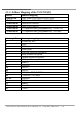
The user-defined pins of the 7521 family are given as follows:
User defined pins Reconfiguration pins Customized I/O pins
7521(D) 3 5 3+5=8
7522(D)/7522A(D)/
7523(D)/7524(D)/
7527(D)
0 0 0+0=0
7521/2/2A/3/4/7 Series Hardware User’s Manual, Ver. 1.5 Sep/2002, 7Mh-001-15 -----43