
User Manual


7521/2/2A/3/4/7 Series Hardware User’s Manual, Ver. 1.5 Sep/2002, 7Mh-001-15 -----16
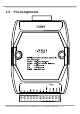
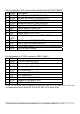
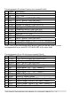
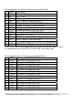
Pin assignment of bottom 14-pin screw terminal block:
Pin Name Description
1 DO 100 mA, 30V max.
2 DI 3.5V ~ 30V
3 D1+ DATA+ pin of COM1 (RS-485)
4 D1- DATA - pin of COM1 (RS-485)
5 CTS1 Clear To Send of COM1 (RS-232)
6 RTS1 Request To Send of COM1 (RS-232)
7 GND Signal ground of RS-232
8 TXD1 Transmits Data of COM1 (RS-232)
9 RXD1 Receives Data of COM1 (RS-232)
10 INIT* Initial pin, 3.5V ~ 30V
11 D2+ DATA+ pin of COM2 (RS-485)
12 D2- DATA - pin of COM2 (RS-485)
13 +VS V+ of power supply (+10 to +30VDC unregulated)
14 GND GND of power supply
Note: The COM1 can be used as a RS-232 port or a RS-485 port. It is not
recommended to use both RS-232 & RS-485 at the same time.
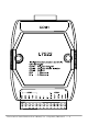
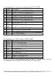
Pin assignment of top 14-pin screw terminal block:
15 TXD3+ TXD+ pin of COM3 (RS-422/RS-485)
16 TXD3- TXD - pin of COM3 (RS-422/RS-485)
17 RXD3+ RXD+ pin of COM3 (RS-422)
18 RXD3- RXD - pin of COM3 (RS-422)
19 DI0 Digital Input, 3.5V ~ 30V, channel 0
20 DI1 Digital Input, 3.5V ~ 30V, channel 1
21 DI2 Digital Input, 3.5V ~ 30V, channel 2
22 DI3 Digital Input, 3.5V ~ 30V, channel 3
23 GND GND of Digital Output
24 PWR Power of Digital Output
25 DO0 Digital Output, 100 mA, 30V max., channel 0
26 DO1 Digital Output, 100 mA, 30V max., channel 1
27 DO2 Digital Output, 100 mA, 30V max., channel 2
28 DO3 Digital Output, 100 mA, 30V max., channel 3