EM78P312N 8-BIT Microcontroller Green Product Specification DOC. VERSION 1.0 ELAN MICROELECTRONICS CORP.
Trademark Acknowledgments: IBM is a registered trademark and PS/2 is a trademark of IBM. Windows is a trademark of Microsoft Corporation. ELAN and ELAN logo are trademarks of ELAN Microelectronics Corporation. Copyright © 2006 by ELAN Microelectronics Corporation All Rights Reserved Printed in Taiwan The contents of this specification are subject to change without further notice. ELAN Microelectronics assumes no responsibility concerning the accuracy, adequacy, or completeness of this specification.
Contents Contents 1 2 3 4 5 General Description.....................................................................................................1 Features ........................................................................................................................1 Pin Assignment ............................................................................................................1 Pin Description.........................................................................................
Contents 5.14 Reset and Wake-up............................................................................................ 42 5.14.1 5.14.2 5.14.3 5.14.4 Reset ................................................................................................................ 42 Wake-up from Sleep Mode ............................................................................... 43 Wake-up from Idle Mode ..................................................................................
EM78P312N 8-Bit Microcontroller 1 General Description The EM78P312N is an 8-bit microprocessor with low-power, high-speed CMOS technology and high noise immunity. It has an on-chip 4K×13-bits Electrical One Time Programmable Read Only Memory (OTP-ROM). It provides multi-protection bits to prevent intrusion of user’s OTP memory codes. Seven Option bits are also available to meet user’s requirements.
EM78P312N 8-Bit Microcontroller 4 Pin Description Table 1 Symbol VDD Pin No. Type 28 − Power supply Crystal type: Crystal input terminal RC type: RC oscillator input pin OSCI 2 I OSCO 1 I/O /RESET 27 I P60~P67 P70~P73 19~26 15~18 Function Crystal type: Output terminal for crystal oscillator RC type: Instruction clock output External clock signal input Input pin with Schmitt Trigger. If this pin remains at logic low, the controller will also remain in reset condition.
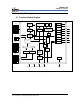
EM78P312N 8-Bit Microcontroller 5 Function Description 5.1 Functional Block Diagram P9 P90 P91 P92 P93 P94 P95 P96 P97 Ext. OSC. PC ROM Ext. RC Start-up Timer WDT TC2 Instruction Register Oscillation Generation 8-level stack (13 bit) TC2 TC3 TC3 TC4 Reset Instruction Decoder P8 TC4 TX RX UART SPI P80 P81 Mux . ALU TCC Sin Sout SCK TCC Keytone TBKTC P7 P70 P71 P72 P73 P74 P75 P76 P77 R4 RAM ACC R3 Status Reg.
EM78P312N 8-Bit Microcontroller 5.
EM78P312N 8-Bit Microcontroller R0 (Indirect Addressing Register) R0 is not a physically implemented register. Its major function is to act as an indirect addressing pointer. Any instruction using R0 as a pointer actually accesses data pointed by the RAM Select Register (R4). R1 (Time Clock /Counter) This register is writable and readable just like the other registers. The contents of the prescaler counter are cleared only when a value is written into the TCC register.
EM78P312N 8-Bit Microcontroller R5 PC A12 A11 A10 A9 A8 CALL RET RETL RETI 000 : PAGE0 0000~03FF 001 : PAGE1 0400~07FF 010 : PAGE2 0800~0BFF A7 ~ A0 Store ACC, R3, R5 Reset Vector 0000h WDT Timer Overflow 0003h External INT0 Pin Interrupt Occurs 0006h TCC Overflow 0009h External INT1 pin Interrupt Occurs 000Fh Time Base Timer Interrupt 0012h UART Transmit Data Buffer Empty 0015h UART Receive Data Buffer Full 0018h UART Receive Error 001Bh TC3 Interrupt 0021h SPI Interrupt 0
EM78P312N 8-Bit Microcontroller Bit 3 (P): Power down bit. Set to “1” during power on or by a "WDTC" command and reset to “0” by a "SLEP" command. Bit 2 (Z): Zero flag. Set to "1" if the result of an arithmetic or logic operation is zero.
EM78P312N 8-Bit Microcontroller R6 (Port 6 I/O Data Register) Bit 7 Bit 6 Bit 5 Bit 4 Bit 3 Bit 2 Bit 1 Bit 0 P67 P66 P65 P64 P63 P62 P61 P60 Bit 7 ~ Bit 0 ( P67 ~ P60 ) : 8-bit Port 6 I/O data register User can use IOC6 register to define each bit whether input or output.
EM78P312N 8-Bit Microcontroller Bit 4 ~ Bit 2 ( TC4CK2 ~ TC4CK 0 ) : Timer/Counter 4 Clock Source Select TC4CK2 TC4CK1 TC4CK0 0 0 0 0 0 0 1 0 1 1 0 Clock Source Resolution Max. Time ( Normal, Idle ) ( Fosc=8M ) ( Fosc=8M ) 256μS 65mS 16μS 4mS 4μS 1mS 1μS 255μS 500nS 127.5μS 11 Fc/2 7 1 Fc/2 5 0 Fc/2 3 1 Fc/2 2 0 Fc/2 1 1 0 1 Fc/2 250nS 63.8μS 1 1 0 Fc 125nS 31.
EM78P312N 8-Bit Microcontroller RE (Interrupt Status Flag Register 1) Bit 7 Bit 6 Bit 5 Bit 4 Bit 3 Bit 2 Bit 1 Bit 0 EXIF5 TCIF2 ADIF 0 EXIF3 TCIF4 SPIF TCIF3 Bit 7 ( EXIF5 ) : External Interrupt Flag (/INT5), flag cleared by software. Bit 6 ( TCIF2 ) : 16-bit Timer/Counter 2 Interrupt Flag, flag cleared by software. Bit 5 ( ADIF ) : AD conversion complete flag, flag cleared by software. Bit 3 ( EXIF3 ) : External Interrupt Flag (/INT3), flag cleared by software.
EM78P312N 8-Bit Microcontroller z ISFR2 can be cleared by instruction, but cannot be set by instruction z IMR2 is the interrupt mask register z Note that reading ISFR2 will obtain the result of the ISFR2 "logic AND" and IMR2 Bank 1 R5 TC3CR (Timer/Counter 3 Control Register) Bit 7 Bit 6 Bit 5 Bit 4 Bit 3 Bit 2 Bit 1 Bit 0 TC3CAP TC3S TC3CK1 TC3CK0 TC3M 0 0 0 Bit 7 ( TC3CAP ) : Software capture control TC3CAP = “0” : TC3CAP = “1” : Software capture Bit 6 ( TC3S ) : Timer/Counter 3 star
EM78P312N 8-Bit Microcontroller Bank 1 R8 TC2CR/ ADDL (Timer/Counter 2 Control Register, AD Low 2 bits Data Buffer) Bit 7 Bit 6 Bit 5 Bit 4 Bit 3 Bit 2 Bit 1 Bit 0 ADD1 ADD0 0 TC2M TC2S TC2CK2 TC2CK1 TC2CK0 Bit 7 ~ Bit 6 ( ADD1 ~ ADD0 ) : AD low 2-bit data buffer Bit 4 ( TC2M ) : Timer/Counter 2 mode select TC2M = “0” : Timer/counter mode TC2M = “1” : Window mode Bit 3 ( TC2S ) : Timer/Counter 2 start control TC2S = “0” : Stop and counter clear TC2S = “1” : Start Bit 2 ~ Bit 0 ( TC2CK2 ~ TC
EM78P312N 8-Bit Microcontroller Bit 6 ( ADRUN ) : AD Conversion start ADRUN = “0” : Reset on completion of the conversion by hardware, this bit cannot be reset by software. ADRUN = “1” : Conversion starts Bit 5~ Bit 4 ( ADCK1 ~ ADCK0 ) : AD Conversion Time Select Clock Source ( Normal, Idle ) Max.
EM78P312N 8-Bit Microcontroller Bank 1 RE TBKTC (TBT/Keytone Control) Bit 7 Bit 6 Bit 5 Bit 4 Bit 3 Bit 2 Bit 1 Bit 0 TEN TCK1 TCK0 0 TBTEN TBTCK2 TBTCK1 TBTCK0 Bit 7 ( TEN ) : Keytone enable control TEN = “0” : Disable TEN = “1” : Enable Bit 6 ~ Bit 5 ( TCK1 ~ TCK0 ) : Keytone Output Clock Source Select Clock Source ( Normal, Idle ) TCK1 TCK0 0 0 Fc/2 0 1 Fc/2 1 0 Fc/2 1 1 Keytone Output Frequency ( Fc = 8MHz ) 13 0.976kHz 12 1.953kHz 11 3.906kHz 10 7.
EM78P312N 8-Bit Microcontroller Bit 4 ~ Bit 2 ( BRATE2 ~ BRATE1 ) : Transmit Baud Rate Select BRATE2 BRATE1 BRATE0 Baud Rate e.g. Fc=8MHz 0 0 0 Fc/13 38400 0 0 1 Fc/26 19200 0 1 0 Fc/52 9600 0 1 1 Fc/104 4800 1 0 0 Fc/208 2400 1 0 1 Fc/416 1200 1 1 0 TC4 - 1 1 1 reserved - Bit 1 ( UTBE ): UART transfer buffer empty flag. Set to 1 when transfer buffer is empty. Reset to 0 automatically when writing into the URTD register.
EM78P312N 8-Bit Microcontroller Bit 6 ( EVEN ) : Select parity check EVEN = “0” : Odd parity EVEN = “1” : Even parity Bit 5 ( PRE ) : Enable parity addition PRE = “0” : Disable PRE = “1” : Enable Bit 4 ( PRERR ) : Parity error flag. Set to 1 when parity error occurred, and cleared to 0 by software. Bit 3 ( OVERR ) : Overrun error flag. Set to 1 when overrun error occurred, and cleared to 0 by software. Bit 2 ( FMERR ) : Framing error flag. Set to 1 when framing error occurred, and cleared to 0 by software.
EM78P312N 8-Bit Microcontroller In using the external clock, data input sample is fixed at the middle of data output time. Bit 6 ( DCOL ) : SPI Data collision. DCOL = “0” : No occurrence of Data collision DCOL = “1” : Data collision occurred. It should be cleared by software. Bit 5 ~ Bit 3 ( BRS0 ~ BRS2 ) : SPI Clock Source Select BRS2 BRS1 0 BRS0 0 0 ( Fc = 8MHz ) 0.95Kbit/s 11 3.8Kbit/s 10 7.6Kbit/s 8 30.5Kbit/s 6 122Kbit/s 5 Fc/2 0 1 13 Fc/2 1 1 0 Max.
EM78P312N 8-Bit Microcontroller Bit 2 ~ Bit 1 ( SPIM1 ~ SPIM0) : SPI Transfer Mode Select TC2CK1 TC2CK0 Transfer Mode 0 0 8-bit Transmit/Receive mode 0 1 8-bit Transmit mode 1 0 8-bit Receive mode 1 1 Reserved Bit 0 ( RBF ) : Set to 1 by Buffer Full Detector, and cleared to 0 automatically when reading data from the SPID register. RBF bit will be cleared by hardware when enabling SPI. And RBF bit is read-only.
EM78P312N 8-Bit Microcontroller Bank 3 RC PHC2 (Pull High Control Register 2) Bit 7 Bit 6 Bit 5 Bit 4 Bit 3 Bit 2 Bit 1 Bit 0 - - - - /PHE73 /PHE72 /PHE71 /PHE70 Bit 3 ~ 0 ( /PHE73 ~ /PHE70 ) : Bits 3 ~ 0 of Port 7 Pull high enable bit /PHE7x = “0” : Enable P7x pull high /PHE7x = “1” : Disable P7x pull high Bank 3 RD PLC2 (Pull Low Control Register 2) Bit 7 Bit 6 Bit 5 Bit 4 Bit 3 Bit 2 Bit 1 Bit 0 - - - - /PLE73 /PLE72 /PLE71 /PLE70 Bit 3 ~ 0 ( /PLE73 ~ /PLE70 ) : Bits 3 ~
EM78P312N 8-Bit Microcontroller Bit 2 ( PSR2 ) ~ Bit 0 ( PSR0 ) : TCC prescaler bits PSR2 PSR1 PSR0 Operating Mode 0 0 0 1:2 0 0 1 1:4 0 1 0 1:8 0 1 1 1:16 1 0 0 1:32 1 0 1 1:64 1 1 0 1:128 1 1 1 1:256 IOC6 ~ IOC9 − I/O Port Control Register "1" puts the relative I/O pin into high impedance, while "0" defines the relative z I/O pin as output. IOC6 and IOC9 registers are both readable and writable.
EM78P312N 8-Bit Microcontroller External Interrupt INT Pin Secondary Function Pin Enable Condition /INT0 INT1 P60 P61 ENI + INT0EN (IOCB) ENI + EXIE1 (IMR2) INT3 P80, TC3 ENI + EXIE3 (IMR2) Rising or Falling or Rising/Falling 7/Fc /INT5 P73, /SLEEP ENI + EXIE5 (IMR2) - - Digital Noise Reject Edge Falling Rising or Falling 15/Fc, 63/Fc ADOSCR − AD Offset Control Register ( Address : 0Ch ) Bit 7 Bit 6 Bit 5 Bit 4 Bit 3 Bit 2 Bit 1 Bit 0 CALI SIGN VOF[2] VOF[1] VOF[0] 0 0 0
EM78P312N 8-Bit Microcontroller Bit 1 ( SPIE ) : SPI Interrupt enable bit. SPIE = “0” : disable SPIF interrupt SPIE = “1” : enable SPIF interrupt Bit 0 ( TCIE3 ) : Timer/Counter 3 Interrupt enable bit. TCIE3 = “0” : disable TCIF3 interrupt TCIE3 = “1” : enable TCIF3 interrupt Individual interrupt is enabled by setting its associated control bit in the IMR1 to "1". Global interrupt is enabled by the ENI instruction and is disabled by the DISI instruction. The IMR1 register is both readable and writable.
EM78P312N 8-Bit Microcontroller 5.
EM78P312N 8-Bit Microcontroller In Sleep mode, the internal oscillator is turned off and all system operation is halted. Sleep mode is released by /SLEEP pin (level sensitive or edge sensitive can be set by System Control Register (SCR) Bit 0 (REM)). After a warm-up period, the next instruction will be executed which is after the Sleep mode start instruction. Sleep mode can also be released by setting the /RESET pin to low and executing a reset operation.
EM78P312N 8-Bit Microcontroller AD7 (P97) AD6 (P96) VDD 8 to 1 Analog switch AD5 (P95) AD4 (P94) AD3 (P93) AD2 (P92) VREF ADC (Successive Approximation) Power Down Start to Convert Fosc/4 AD1 (P91) Fosc/16 Fosc/32 4 to 1 MUX AD0 (P90) 7-0 ADIC 2 1 0 ADCR 5 4 ADCR 5 5 ISFR1 9 8 7 6 5 4 3 2 1 0 IMR1 6 3 7 ADCR DATA BUS Fig. 5-5 AD Converter It is a 10-bit successive approximation type AD converter.
EM78P312N 8-Bit Microcontroller 5.
EM78P312N 8-Bit Microcontroller 23 Fosc/2 21 Fosc/2 16 Fosc/2 14 Fosc/2 13 Fosc/2 MUX Falling Edge Detector 12 Fosc/2 TBT Interrupt 11 Fosc/2 Fosc/2 9 TBTEN TBTCK2:0 3 TBKTC Fig. 5-8 TBT Configuration The Time Base Timer is used to generate the base time for key scan or dynamic display processing. The interrupt is generated in the first falling edge of the source clock after TBTEN is set to “1”. Source Clock TBTEN TBT Interrupt Fig.
EM78P312N 8-Bit Microcontroller 5.
EM78P312N 8-Bit Microcontroller The figure below shows the general format of one character sent or received. The communication channel is normally held in the marked state (high). Character transmission or reception starts with a transition to the space state (low). The first bit transmitted or received is the start bit (low). It is followed by the data bits, in which the least significant bit (LSB) comes first. The data bits are followed by the parity bit.
EM78P312N 8-Bit Microcontroller 3. Start transmitting. 4. Serially transmitted data are transmitted in the following order from the TX pin. 5. Start bit: one “0” bit is output. 6. Transmit data: 7, 8 or 9 bits data are output from the LSB to the MSB. 7. Parity bit: one parity bit (odd or even selectable) is output. 8. Stop bit: one “1” bit (stop bit) is output. Mark state: output “1” continues until the start bit of the next transmitted data.
EM78P312N 8-Bit Microcontroller 5.
EM78P312N 8-Bit Microcontroller 5.8.1 Serial Clock Six internal clocks can be selected by setting BRS0 ~ BRS2 and the clock output to the outside from /SCK (P70) pin. The External clock can also be used and connected to /SCK (P70) pin. 5.8.2 Shift Direction and Sample Phase Setting up the DORD bit of the SPIC1 register can determine the shift direction. Setting up the EDS bit of the SPIC1 register can select the rising edge or falling edge and latch the data.
EM78P312N 8-Bit Microcontroller (b) 8-bit Receive Mode Setting SPIM0 ~ SPIM1 to receive mode and setting SPIS to “1” to start receiving. The data are input sequentially from the SI pin in synchronous with the serial clock. When the final bit of transfer data has been received, the SPI interrupt is generated and SPIS is cleared to “0” by hardware. In order to receive the next data, the SPIS must be set to “1” again by software.
EM78P312N 8-Bit Microcontroller shift start shift start SPIS RBF shift finish WBE shift finish /SCK pin SO pin a0 a1 a2 a3 a4 a5 a6 a7 b0 b1 b2 b3 b4 b5 b6 b7 SI pin c0 c1 c2 c3 c4 c5 c6 c7 d0 d1 d2 d3 d4 d5 d6 d7 SPIF SPID a c write data d b read data write data read data Fig. 5-16 Transmit/Receive Mode (8-bit, 1 word) (d) Multiple Device Connect (/SS) When selecting external clock for transfer clock source, the /SS function can be used.
EM78P312N 8-Bit Microcontroller 5.
EM78P312N 8-Bit Microcontroller 5.9.1 Timer Mode In Timer mode, counting up is performed using the internal clock. When the contents of the up-counter matched with the TCR2 (TCR2H+TCR2L), then interrupt is generated and the counter is cleared. Counting up resumes after the counter is cleared. Internal clock Up-counter 0 TCR2 1 2 3 4 5 n-3 n-2 n-1 n 0 n 2 1 3 counter clear match TC2 interrupt Fig. 5-19 Timer Mode Timing Chart 5.9.
EM78P312N 8-Bit Microcontroller TC2 pin Internal clock Up-counter 0 TCR2 1 2 n-3 n-1 n-2 n match n 0 1 2 3 counter clear TC2 interrupt Fig. 5-21 Window Mode Timing Chart 5.
EM78P312N 8-Bit Microcontroller INT3ES Edge Detector Rising Inhibit Falling Capture Control TC3 Interrupt TC3M TC3 pin M fc/2 , fs/2 10 2 fc/2 , fs/2 7 fc/2 12 4 MUX 8-bit Up-counter Overflow TC3S TC2CK Comparator CAP 2 Capture Capture TC3CR TCR3B TCR3A Fig. 5-22 Configuration of Timer/Counter3 5.10.1 Timer Mode In Timer mode, counting up is performed using the internal clock.
EM78P312N 8-Bit Microcontroller of the TC3 pin input, the contents of the counter are loaded into TCR3A, counter is cleared and interrupt is generated again. If an overflow before the edge is detected, the FFH is loaded into TCR3DA and an overflow interrupt is generated. During interrupt processing, it can be determined whether or not there is an overflow by checking whether the TCR3DA value is FFH.
EM78P312N 8-Bit Microcontroller TC4FF TC4M (1,1) 11 fc/2 7 fc/2 3 fc/2 TC4 pin Clear MUX TC4 Interrupt F/F Clear Set Q Toggle TC4M(1,*) 8-bit Up-counter /PWM, /PDO Pin Overflow Match Comparator TC4CK 3 TC4S TCR4 TC4CR Fig. 5-24 Timer/Counter 4 Configuration 5.11.1 Timer Mode In Timer mode, counting up is performed using the internal clock. When the contents of the up-counter matched with the TCR4, then interrupt is generated and the counter is cleared.
EM78P312N 8-Bit Microcontroller 5.11.4 PWM Mode In Pulse Width Modulation (PWM) Output mode, counting up is performed using the internal clock. The contents of the TCR4 are compared with the contents of the up-counter. The F/F is toggled when match is found. The counter is still counting, the F/F is toggled again when the counter overflows, then the counter is cleared. The F/F output is inverted and output to the /PWM pin. A TC4 interrupt is generated each time an overflow occurs.
EM78P312N 8-Bit Microcontroller 5.13 I/O Ports The I/O registers, Port 6, Port 7, Port 8, and Port 9 are bi-directional tri-state I/O ports. Each I/O pin can be defined as “input” or “output” pin by the I/O control register (IOC6 ~ IOC9). The I/O registers and I/O control registers are both readable and writable. The I/O interface circuits for Port 6, Port 7, Port 8, and Port 9 are shown in Fig. 5-26. PCRD Q PORT 0 1 P R D CLK Q C L Q P R Q C CLK L PCW R IOD D M U X PDW R PDRD Fig.
EM78P312N 8-Bit Microcontroller The Watchdog timer and prescaler are cleared. Upon power on, the upper two bits of R3 are cleared. Upon power on, the upper two bits of R4 are cleared. Upon power on, the upper three bits of R5 are cleared. The bits of CONT register are set to all “1” except Bit 6 (INT flag). ISFR0, ISFR1, ISFR2 register and IMR1, IMR2 registers are cleared. The controller has two modes for power saving. (1) SLEEP mode: R5 (SIS) = 1, SLEP instruction.
EM78P312N 8-Bit Microcontroller Table 6.
EM78P312N 8-Bit Microcontroller Register Bank 0 Address Name 0x05 0x06 0x07 0x08 0x09 SCR Port 6 Port 7 Port 8 Port 9 Reset Type Bit 7 Bit 6 Bit 5 Bit 4 Bit Name X X X PS0 Power-on U 0 0 0 /RESET and WDT time out U 0 0 0 Wake-up from Sleep, Idle mode U P P Bit Name P67 P66 Power-on 1 1 /RESET and WDT time out 1 Wake-up from Sleep, Idle mode P TC4CR 0X0D 0X0E 0X0F TC4D ISFR0 ISFR1 ISFR2 Bit 1 Bit 0 X X SIS REM U U 0 0 U U 0 0 P U U P P P
EM78P312N 8-Bit Microcontroller Register Bank 1 Addres s 0x05 Name TC3CR Reset Type Bit 7 Bit 6 Bit Name TC3CAP TC3S Power-on 0 0 TC3DA TC3DB 0x0C 0X0D 0X0E 46 • ADCR ADIC ADDH TBKTC X X U U 0 0 0 U U U P P U U U TC3DA7 TC3DA6 TC3DA5 TC3DA4 TC3DA3 TC3DA2 TC3DA1 TC3DA0 Power-on 0 0 0 0 0 0 0 /RESET and WDT time out 0 0 0 0 0 0 0 0 Wake-up from Sleep, Idle mode P P P P P P P P 0 TC3DB7 TC3DB6 TC3DB5 TC3DB4 TC3DB3 TC3DB2 TC3DB1 TC3DB0 Power-on
EM78P312N 8-Bit Microcontroller Register Bank 2 Address Name Reset Type Bit Name 0x05 0x06 URC1 URC2 URS URRD URTD Bit 4 Bit 3 Bit 2 Bit 1 Bit 0 URTD8 UMODE1 UMODE0 BRATE2 BRATE1 BRATE0 UTBE TXE 0 0 0 0 0 0 /RESET and WDT time out P P P P P P 0 0 Wake-up from Sleep, Idle mode P 0 P P P P P 0 Bit Name X X Power-on U U SBIM1 SBIM0 UINVEN 0 0 0 0 X X X U U U /RESET and WDT time out U U P P P U U U Wake-up from Sleep, Idle mode U U P P P U
EM78P312N 8-Bit Microcontroller General Purpose Registers Address Name 0x10 R10 ~ ~ 0x3F R3F Reset Type Bit 7 Bit 6 Bit 5 Bit 4 Bit 3 Bit 2 Bit 1 Bit 0 Bit Name - - - - - - - - Power-on U U U U U U U U /RESET and WDT time out P P P P P P P P Wake-up from Sleep, Idle mode P P P P P P P P Legend: “×” = not used “P” = previous value before reset “u” = unknown or don’t care “t” = check Table 7 5.14.
EM78P312N 8-Bit Microcontroller VDD D CLK Oscillator Q CLK CLR Power-on Reset Voltage Detector WDTE WDT Timeout WDT Setup Time RESET /RESET Fig. 5-28 Controller Reset Block Diagram 5.15 Interrupt The EM78P312N has 15 interrupts (9 external, 6 internal) as listed below: Table 9 Interrupt Vector Interrupt Source Enable Condition Int. Flag Int.
EM78P312N 8-Bit Microcontroller The flag (except ICIF bit) in the Interrupt Status Register (ISFR 2) is set regardless of the status of its mask bit or the execution of ENI. The RETI instruction ends the interrupt routine and enables the global interrupt (the execution of ENI). 5.16 Oscillator 5.16.1 Oscillator Modes The EM78P312N can operate in two different oscillator modes, i.e., Crystal oscillator mode and External RC oscillator mode (ERC) oscillator mode.
EM78P312N 8-Bit Microcontroller Ext. Clock OSCI OSCO EM78P312N EM78P809N Fig. 5-29 Crystal/Resonator Circuit C1 OSCI XTAL EM78P312N EM78P809N OSCO C2 RS Fig. 5-30 Crystal/Resonator Circuit Table12. Capacitor Selection Guide for Crystal Oscillator or Ceramic Resonator Oscillator Type Frequency Mode Ceramic Resonator HXT Crystal Oscillator HXT Frequency C1 (pF) C2 (pF) 2.0 MHz 20~40 20~40 4.0 MHz 10~30 10~30 1.0 MHz 15~30 15~30 2.0 MHz 15 15 4.
EM78P312N 8-Bit Microcontroller 4.7 K OSCI 740 4 EM78P809N EM78P312N 10 K Vdd 740 4 10 K XTAL C1 C2 Fig. 5-32 Crystal/Resonator-Parallel Mode Circuit 5.16.3 External RC Oscillator Mode For applications that do not need very precise timing calculation, the RC oscillator offers a lot of cost savings.
EM78P312N 8-Bit Microcontroller Table13. RC Oscillator Frequencies Cext Average Fosc 5V, 25°C Average Fosc 3V, 25°C Rext 20 pF 100 pF 300 pF 3.3k 5.1k 4.32 MHz 2.83 MHz 3.56 MHz 2.8 MHz 1.57 MHz 10k 1.62 MHz 100k 184kHz 187kHz 3.3k 1.39 MHz 1.35 MHz 5.1k 950kHz 930kHz 10k 500kHz 490kHz 100k 54kHz 55kHz 3.3k 580kHz 550kHz 5.1k 390kHz 380kHz 10k 100k 200kHz 21kHz 200kHz 21kHz 1 Note: : Measured based on DIP packages. 2 : The values are for design reference only. 5.
EM78P312N 8-Bit Microcontroller Bit 4 (OSC) : Oscillator type selection OSC = “0” : RC type OSC = “1” : Crystal type Bit 3 (HLP) : Power selection HLP = “0” : Low power HLP = “1” : High power Bit 2~0 (PR2~PR0) : Protect Bit PR2~PR0 are write-protect bits, configured as follow s: PR2 PR1 PR0 Protect 1 Disable Others 1 Enable 1 5.17.2 Customer ID Register Word 1 Bit 12~Bit 0 XXXXXXXXXXXXX Word 2 Bit 12~Bit 0 XXXXXXXXXXXXX Bits 12 ~ 0: Customer’s ID code 5.
EM78P312N 8-Bit Microcontroller Vdd R /RESET D EM78P312N EM78P809N Rin C Fig. 5-34 External Power-Up Reset Circuit 5.18.2 Residue-Voltage Protection When battery is replaced, device power (VDD) is taken off but residue-voltage remains. The residue-voltage may trip below VDD minimum, but not to zero. This condition may cause a poor power-on reset. Fig.35 and Fig. 36 show how to build the residue-voltage protection circuit. Vdd Vdd 33K EM78P312N EM78P809N Q1 10K /RESET 40K 1N4684 Fig.
EM78P312N 8-Bit Microcontroller 5.19 Instruction Set Each instruction in the instruction set is a 13-bit word divided into an OP code and one or more operands. Normally, all instructions are executed within one single instruction cycle (one instruction consists of 2 oscillator periods), unless the program counter is changed by instruction "MOV R2,A", "ADD R2,A", or by instructions of arithmetic or logic operation on R2 (e.g. "SUB R2,A", "BS(C) R2,6", "CLR R2", ⋅⋅⋅⋅).
EM78P312N 8-Bit Microcontroller Binary Instruction Hex Mnemonic Operation 0 0 0 0 0 0 0 0 0 0 0 0 0 0 0 0 0 0 0 0 0 0 0 0000 0000 0000 0001 0001 0001 0001 0010 0010 0010 0010 0011 0011 0011 0011 0100 0100 0100 0100 0101 0101 0101 0101 01rr 1000 11rr 00rr 01rr 10rr 11rr 00rr 01rr 10rr 11rr 00rr 01rr 10rr 11rr 00rr 01rr 10rr 11rr 00rr 01rr 10rr 11rr rrrr 0000 rrrr rrrr rrrr rrrr rrrr rrrr rrrr rrrr rrrr rrrr rrrr rrrr rrrr rrrr rrrr rrrr rrrr rrrr rrrr rrrr rrrr 00rr 0080 00rr 01rr 01rr 01rr 01rr 02r
EM78P312N 8-Bit Microcontroller 6 Absolute Maximum Ratings 6.1 Absolute Maximum Ratings Items Rating Temperature under bias -40°C to 85°C Storage temperature -65°C to 150°C Input voltage -0.3V to +6.0V Output voltage -0.3V to +6.0V Operating Frequency (2clk) DC to 10MHz 6.2 Recommended Operating Conditions Vss = 0V Symbol Parameter VDD Supply Voltage Fc 58 • Crystal: VDD 4.5 to 5.5V Crystal: VDD 2.5 to 5.5V Condition Min. Typ. Fc = 10MHz 4.0 − Fc = 4MHz 2.
EM78P312N 8-Bit Microcontroller 7 Electrical Characteristics 7.1 DC Electrical Characteristics Ta= 25 °C, VDD= 5.0V ± 5%, VSS= 0V Symbol Parameter Fc ERC Crystal: 4.
EM78P312N 8-Bit Microcontroller Ta= 25 °C, VDD= 3.0V ± 5%, VSS= 0V Symbol Parameter Condition Min. Typ. Max. Unit Fc ERC Crystal: 2.
EM78P312N 8-Bit Microcontroller A/D Converter Characteristic (Vdd =2.5V to 5.5V, Vss=0V, Ta = -40 to 85°C) Symbol VAREF VASS VAI IAI1 IAI2 IVDD Ivref IVDD IVref Parameter Condition Analog reference voltage VAREF - VASS≧2.5V − Analog input voltage Analog supply current Analog supply current Min. Typ. Max. Unit 2.5 − VDD V Vss − Vss V VASS − VAREF V VDD =VAREF=5.0V, VASS =0.0V 750 850 1000 μA (V reference from VDD) -10 0 +10 μA VDD =VAREF=5.0V, VASS =0.
EM78P312N 8-Bit Microcontroller 7.2 AC Electrical Characteristic Ta=- 40°C ~ 85 °C, VDD=5V ± 5%, VSS=0V Symbol Parameter Conditions Min Dclk Input CLK duty cycle − 45 Tins Instruction cycle time Crystal type (high frequency) (CLKS="0") RC type Ttcc TCC input period Tdrh Device reset hold time Ta = 25°C 11.3 Trst /RESET pulse width Ta = 25°C 2000 Twdt Watchdog timer period Ta = 25°C 11.
EM78P312N 8-Bit Microcontroller 7.3 Timing Diagram AC Test Input/Output W aveform 2.4 2.0 0.8 TEST POINTS 2.0 0.8 0.4 AC Testing : Input is driven at 2.4V for logic "1",and 0.4V for logic "0".Tim ing m easurem ents are m ade at 2.0V for logic "1",and 0.8V for logic "0". RESET Tim ing (CLK="0") NOP Instruction 1 Executed CLK /RESET Tdrh TCC Input Tim ing (CLKS="0") Tins CLK TCC Ttcc Product Specification (V1.0) 10.03.
EM78P312N 8-Bit Microcontroller APPENDIX A Package Types: OTP MCU Package Type Pin Count Package Size EM78P312NP DIP 28 600 mil EM78P312NK SDIP 28 400 mil EM78P312NAK SDIP 28 300 mil EM78P312NM SOP 28 300 mil EM78P312NS SSOP 28 209 mil Y/S/J:Green product does not contain hazardous substances. The third edition of Sony SS-00259 standard. Pb content should be less than 100ppm. Pb content to fit in with Sony spec. Part No.