EM78P809N 8-BIT Microcontroller Product Specification DOC. VERSION 1.0 ELAN MCCROELECTRONICS CORP.
Trademark Acknowledgments: IBM is a registered trademark and PS/2 is a trademark of IBM. Windows is a trademark of Microsoft Corporation. ELAN and ELAN logo are trademarks of ELAN Microelectronics Corporation. Copyright © 2005 by ELAN Microelectronics Corporation All Rights Reserved Printed in Taiwan The contents of this specification are subject to change without further notice. ELAN Microelectronics assumes no responsibility concerning the accuracy, adequacy, or completeness of this specification.
Contents Contents 1 General Description ··························································································· 1 2 Features ·············································································································· 1 2.1 CPU········································································································································ 1 2.
Contents 5 Absolute Maximum Ratings ············································································ 63 5.1 Absolute Maximum Ratings ································································································· 63 5.2 Recommended Operating Conditions ·················································································· 63 6 Electrical Characteristics················································································· 64 6.
EM78P809N 8-Bit Microcontroller 1 General Description The EM78P809N is an 8-bit microprocessor with low-power, high-speed CMOS technology and high noise immunity. It has a built-in 8K×13-bits Electrical One Time Programmable Read Only Memory (OTP-ROM). It provides multi-protection bits to prevent intrusion of user’s OTP memory codes. Seven Option bits are also available to meet user’s requirements.
EM78P809N 8-Bit Microcontroller 16 bits Counter/Timer z TC2: Timer/Counter/Window 8 bits Timer/Counter z TCC: 8-bit real time clock/counter with overflow interrupt z TC3: Timer/Counter/Capture z TC4: Timer/Counter/ PWM (pulse width modulation)/PDO (Programmable divider output) Time Base Timer: (1Hz ~16kHz at 8MHz) Key tone output: (1kHz ~ 8kHz at 8MHz) Serial transmitter/receiver interface z z Serial Peripheral Interface (SPI): Three-wire synchronous communication Universal asynchr
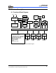
EM78P809N 8-Bit Microcontroller 3 Pin Assignment (ACLK) OSCO OSCI TEST (AD0) P90 (AD1) P91 (AD2) P92 (AD3) P93 (AD4) P94 (AD5) P95 (AD6) P96 (AD7/VREF) P97 (TC3, INT3) P80 (TC4, /PWM, /PDO) P81 VSS 1 2 3 4 5 6 7 8 9 10 11 12 13 14 28 27 26 25 24 23 22 21 20 19 18 17 16 15 VDD /RESET (VPP) P67 (DINCK) P66 (DATAIN) P65 (PGMB) P64 (/SS)(OEB) P63 (/TONE) P62 (TC2) P61 (INT1) P60 (/INT0) P73 (/SLEEP, /INT5) P72 (TX,SO) P71(RX,SI) P70 (/SCK) EM78P809N Fig. 1.
EM78P809N 8-Bit Microcontroller Symbol Pin No.
EM78P809N 8-Bit Microcontroller 4 Function Description 4.
EM78P809N 8-Bit Microcontroller 4.
EM78P809N 8-Bit Microcontroller R0/IAR − Indirect Addressing Register ( Address: 00h ) R0 is not a physically implemented register. Its major function is to act as an indirect addressing pointer. Any instruction using R0 as a pointer actually accesses data pointed by the RAM Select Register (R4). R1/TCC − Time Clock /Counter ( Address: 01h ) This register is writable and readable just like the other registers.
EM78P809N 8-Bit Microcontroller R5 PC A12 A11 A10 A9 A8 001 : PAGE1 0400~07FF 010 : PAGE2 0800~0BFF ~ A0 0000h WDT Timer Overflow 0003h External INT0 Pin Interrupt Occurs 0006h TCC Overflow 0009h STACK LEVEL 3 External INT1 pin Interrupt Occurs 000Fh STACK LEVEL 4 Time Base Timer Interrupt 0012h STACK LEVEL 6 UART Transmit Data Buffer Empty 0015h STACK LEVEL 7 UART Receive Data Buffer Full 0018h UART Receive Error 001Bh TC3 Interrupt 0021h SPI Interrupt 0024h TC4 Interrupt
EM78P809N 8-Bit Microcontroller Bit 3 (P) : Power down bit. Set to “1” during power on or by a "WDTC" command and reset to “0” by a "SLEP" command. Bit 2 (Z) : Zero flag. Set to "1" if the result of an arithmetic or logic operation is zero.
EM78P809N 8-Bit Microcontroller PS2 PS1 PS0 Program Memory Page [Address] 0 0 0 Page 0 [0000~03FF] 0 0 1 Page 1 [0400~07FF] 0 1 0 Page 2 [0800~0BFF] 0 1 1 Page 3 [0C00~0FFF] 1 0 0 Page 4 [1000~13FF] 1 0 1 Page 5 [1400~17FF] 1 1 0 Page 6 [1800~1BFF] 1 1 1 Page 7 [1C00~1FFF] Bit 1 ( SIS ) : SLEEP and IDLE mode select. SIS = “0” : IDLE mode SIS = “1” : SLEEP mode Bit 0 ( REM ) : Release method for sleep mode.
EM78P809N 8-Bit Microcontroller PORT9 − Port 9 I/O Data Register ( Address: 09h ) Bit 7 Bit 6 Bit 5 Bit 4 Bit 3 Bit 2 Bit 1 Bit 0 P97 P96 P95 P94 P93 P92 P91 P90 Bit 7 ~ Bit 0 ( P97 ~ P90 ) : 8-bit Port 97 ~ Port 90 I/O data register User can use IOC9 register to define each bit whether input or output.
EM78P809N 8-Bit Microcontroller TC4D − Timer 4 Data Buffer ( Address: 0Ch ) Bit 7 Bit 6 Bit 5 Bit 4 Bit 3 Bit 2 Bit 1 Bit 0 TC4D7 TC4D6 TC4D5 TC4D4 TC4D3 TC4D2 TC4D1 TC4D0 Bit 7 ~ Bit 0 ( TC4D7 ~ TC4D0 ) : Data buffer of 8-bit Timer/Counter 4. ISFR0 − Interrupt Status Flag Register 0 and INT3 Edge Detect Flag. ( Address : 0Dh ) Bit 7 Bit 6 Bit 5 Bit 4 Bit 3 Bit 2 Bit 1 Bit 0 0 0 INT3F INT3R 0 0 WDTIF EXIF0 Bit 5 ( INT3F ) : External interrupt 3 falling edge detect flag.
EM78P809N 8-Bit Microcontroller ISFR2 − Interrupt Status Flag Register 2 ( Address: 0Fh ) Bit 7 Bit 6 Bit 5 Bit 4 Bit 3 Bit 2 Bit 1 Bit 0 0 UERRIF RBFF TBEF TBIF EXIF1 0 TCIF0 Bit 6 (UERRIF) : UART Receiving Error Interrupt, cleared by software or UART disabled. Bit 5 (RBFF) : UART Receive Mode Data Buffer Full Interrupt Flag. Flag cleared by software. Bit 4 (TBEF) : UART Transmit Mode Data Buffer Empty Interrupt Flag. Flag cleared by software. Bit 3 (TBIF) : Time Base Timer Interrupt Flag.
EM78P809N 8-Bit Microcontroller Bit 5 ~ Bit 4 ( TC3CK1 ~ TC3CK0 ) : Timer/Counter3 Clock Source Select TC3CK1 TC3CK0 0 0 Clock source Resolution Max. time ( Normal, Idle ) ( Fc=8M ) ( Fc=8M ) 12 512μS 131.1mS 10 Fc/2 0 1 Fc/2 128μS 32.6mS 1 0 Fc/27 16μS 4.
EM78P809N 8-Bit Microcontroller Bit 2 ~ Bit 0 ( TC2CK2 ~ TC2CK0 ) : Timer/Counter 2 Clock Source Select TC2CK2 TC2CK1 TC2CK0 0 0 0 Clock Source Resolution Max. Time ( Normal, Idle ) ( Fc=8M ) ( Fc=8M ) 23 1.05s 19.1h 13 1.02ms 1.1min 8 32μs 2.1s 3 Fc/2 0 0 1 Fc/2 0 1 0 Fc/2 0 1 1 Fc/2 1μs 65.5ms 1 0 0 Fc 125ns 7.
EM78P809N 8-Bit Microcontroller Bit 5~ Bit 4 ( ADCK1 ~ ADCK0 ) : AD Conversion Time Select Clock Source ( Normal, Idle ) Max.
EM78P809N 8-Bit Microcontroller TBKTC − TBT/Keytone Control ( Address: 0Eh ) Bit 7 Bit 6 Bit 5 Bit 4 Bit 3 Bit 2 Bit 1 Bit 0 TEN TCK1 TCK0 0 TBTEN TBTCK2 TBTCK1 TBTCK0 Bit 7 ( TEN ) : Keytone enable control TEN = “0” : Disable TEN = “1” : Enable Bit 6 ~ Bit 5 ( TCK1 ~ TCK0 ) : Keytone Output Clock Source Select TCK1 TCK0 0 0 Clock Source Keytone Output Frequency ( Normal, Idle ) ( Fc = 8MHz ) 13 0.976kHz 12 1.953kHz 11 3.906kHz 10 7.
EM78P809N 8-Bit Microcontroller Bit 6 ~ Bit 5 ( UMODE1 ~ UMODE0 ) : UART Transmission Mode Select Bit UMODE1 UMODE0 UART Mode 0 0 Mode1: 7-bits 0 1 Mode2: 8-bits 1 0 Mode3: 9-bits 1 1 Reserved Bit 4 ~ Bit 2 ( BRATE2 ~ BRATE1 ) : Transmit Baud Rate Select BRATE2 BRATE1 BRATE0 Baud Rate e.g.
EM78P809N 8-Bit Microcontroller URS − UART Status Register ( Address: 07h ) Bit 7 Bit 6 Bit 5 Bit 4 Bit 3 Bit 2 Bit 1 Bit 0 URRD8 EVEN PRE PRERR OVERR FMERR URBF RXE Bit 7 ( URRD8 ) : Receiving data bit 8 Bit 6 ( EVEN ) : Select parity check EVEN = “0” : Odd parity EVEN = “1” : Even parity Bit 5 ( PRE ) : Enable parity addition PRE = “0” : Disable PRE = “1” : Enable Bit 4 ( PRERR ) : Parity error flag. Set to 1 when parity error occurred, and cleared to 0 by software.
EM78P809N 8-Bit Microcontroller URTD − UART Transmit Data Buffer ( Address: 09h ) Bit 7 Bit 6 Bit 5 Bit 4 Bit 3 Bit 2 Bit 1 Bit 0 URTD 7 URTD 6 URTD 5 URTD 4 URTD 3 URTD 2 URTD 1 URTD0 Bit 7 ~ Bit 0 ( URTD 7 ~ URTD 0) : UART transmit data buffer. Write only. Register Bank 3 ( R3 bits ( 7,6) = (1,1) ) SPIC1 − SPI Control Register 1 ( Address: 05h ) Bit 7 Bit 6 Bit 5 Bit 4 Bit 3 Bit 2 Bit 1 Bit 0 SMP DCOL BRS2 BRS1 BRS0 EDS DORD WBE Bit 7 ( SMP ) : SPI data input sample phase.
EM78P809N 8-Bit Microcontroller Bit 0 ( WBE ) : Write buffer empty flag. Read only. WBE = “0” : Write buffer empty WBE = “1” : Not empty, set to “1” automatically when writing data to the data buffer. SPIC2 − SPI Control Register 2 (Address : 06h ) Bit 7 Bit 6 Bit 5 Bit 4 Bit 3 Bit 2 Bit 1 Bit 0 SPIS 0 0 0 0 SPIM1 SPIM0 RBF Bit 7 ( SPIS ) : SPI start shift, set the bit to “1” and shift register starts to shift. It is cleared by hardware when shifting is finished.
EM78P809N 8-Bit Microcontroller Bit 3 ~ 0 ( /PHE63 ~ /PHE60 ) : bit 3 ~ 0 of Port 6 Pull high enable bit /PHE6x = “0” : Enable P6x pull high /PHE6x = “1” : Disable P6x pull high PLC1 (Pull Low Control Register 1 ( Address : 0Bh ) Bit 7 Bit 6 Bit 5 Bit 4 Bit 3 Bit 2 Bit 1 Bit 0 - - /PLE81 /PLE80 /PLE63 /PLE62 /PLE61 /PLE60 Bit 5 ~ 4 ( /PLE81 ~ /PLE80 ) : bits 1, 0 of Port 8 Pull low enable bit /PLE8x = “0” : Enable P8x pull low /PLE8x = “1” : Disable P8x pull low Bit 3 ~ 0 ( /PLE63 ~ /PLE60 )
EM78P809N 8-Bit Microcontroller 4.3 Special Purpose Registers A (Accumulator) Internal data transfer, or instruction operand holding. It cannot be addressed. CONT (Control Register) Bit 7 Bit 6 Bit 5 Bit 4 Bit 3 Bit 2 Bit 1 Bit 0 WDTO /INT WDTP1 WDTP0 WDTE PSR2 PSR1 PSR0 CONT register is both readable and writable.
EM78P809N 8-Bit Microcontroller IOC6 ~ IOC9 − I/O Port Control Register "1" puts the relative I/O pin into high impedance, while "0" defines the relative I/O pin as output. IOC6 and IOC9 registers are both readable and writable.
EM78P809N 8-Bit Microcontroller External Interrupt INT Pin Secondary Function Pin Enable Condition Edge Digital Noise Reject Falling - /INT0 P60 ENI + INT0EN (IOCB) INT1 P61 ENI + EXIE1 (IMR2) Rising or Falling 15/Fc, 63/Fc Rising or Falling or Rising/Falling 7/Fc INT3 P80, TC3 ENI + EXIE3 (IMR2) /INT5 P73, /SLEEP ENI + EXIE5 (IMR2) - ADOSCR − AD Offset Control Register ( Address : 0Ch ) Bit 7 Bit 6 Bit 5 Bit 4 Bit 3 Bit 2 Bit 1 Bit 0 CALI SIGN VOF[2] VOF[1] VOF[0] 0 0
EM78P809N 8-Bit Microcontroller Bit 3 ( EXIE3 ) : External INT3 pin Interrupt enable bit. EXIE3 = “0” : disable EXIF3 interrupt EXIE3 = “1” : enable EXIF3 interrupt Bit 2 ( TCIE4 ) : Timer/Counter 4 Interrupt enable bit. TCIE4 = “0” : disable TCIF4 interrupt TCIE4 = “1” : enable TCIF4 interrupt Bit 1 ( SPIE ) : SPI Interrupt enable bit. SPIE = “0” : disable SPIF interrupt SPIE = “1” : enable SPIF interrupt Bit 0 ( TCIE3 ) : Timer/Counter 3 Interrupt enable bit.
EM78P809N 8-Bit Microcontroller Bit 3 ( TBIE ) : Time base timer interrupt enable bit. TBIE = “0” : disable TBIF interrupt TBIE = “1” : enable TBIF interrupt Bit 2 ( EXIE1 ) : External INT 1 Interrupt enable bit. EXIE1 = “0” : disable EXIF1 interrupt EXIE1 = “1” : enable EXIF1 interrupt Bit 0 ( TCIE0 ) : TCC Interrupt enable bit. TCIE0 = “0” : disable TCIF0 interrupt TCIE0 = “1” : enable TCIF0 interrupt Individual interrupt is enabled by setting its associated control bit in the IMR2 to "1".
EM78P809N 8-Bit Microcontroller Table 2. Mode Switching Control Mode Switch Switch Method Note Normal Æ Sleep Set SIS = 1, execute SLEP instruction Sleep Æ Normal /SLEEP pin wake up Normal Æ Idle Set SIS = 0, execute SLEP instruction Idle Æ Normal Interrupt Table 3.
EM78P809N 8-Bit Microcontroller Wake-up Signal 1. Individual interrupt source in IMR1, IMR2 2. WDT interrupt request SLEEP Mode IDLE Mode R5 (SIS) = 1+SLEP Instruction R5 (SIS)= 0 + SLEP Instruction NORMAL Mode R5 (SIS)=(*) 1. Wake-up 2. Jump to an Interrupt vector after RETI Interrupt instruction, then jump to the next instruction or enter IDLE mode No effect (**) 3. /INT0 4. Execute ENI instruction 1. Wake-up 2.
EM78P809N 8-Bit Microcontroller AD7 (P97) AD6 (P96) VDD 8 to 1 Analog switch AD5 (P95) AD4 (P94) AD3 (P93) AD2 (P92) VREF ADC (Successive Approximation) Power Down Start to Convert Fosc/4 AD1 (P91) Fosc/16 Fosc/32 4 to 1 MUX AD0 (P90) 7-0 ADIC 2 1 0 ADCR 5 ADCR 4 5 ISFR1 5 9 8 7 6 5 4 3 2 1 0 IMR1 6 3 7 ADCR DATA BUS Fig. 6. AD Converter It is a 10-bit successive approximation type AD converter.
EM78P809N 8-Bit Microcontroller Table 5 ADCK1:0 Operation Mode Max. Frequency (Fc) Max. Conversion Rate per Bit Max. Conversion Rate 00 Fc/4 1MHz 250kHz (4μs) 48us(20.8kHz) 01 Fc/16 4MHz 250kHz (4μs) 48us(20.8kHz) 10 Fc/32 8MHz 250kHz (4μs) 8us(20.8kHz) 11 Reserved - - - 4.
EM78P809N 8-Bit Microcontroller P63 TEN TONE Pin Fig. 8. TONE Output Pin Timing Chart 23 Fosc/2 21 Fosc/2 16 Fosc/2 14 Fosc/2 13 Fosc/2 MUX Falling Edge Detector 12 Fosc/2 TBT Interrupt 11 Fosc/2 Fosc/2 9 TBTEN TBTCK2:0 3 TBKTC Fig. 9. TBT Configuration Time Base Timer is used to generate the base time for key scan or dynamic display processing. The interrupt is generated in the first falling edge of the source clock after TBTEN is set to “1”. Source Clock TBTEN TBT Interrupt Fig.
EM78P809N 8-Bit Microcontroller 4.
EM78P809N 8-Bit Microcontroller In Universal Asynchronous Receiver Transmitter (UART), each transmitted or received character is individually synchronized by framing it with a start bit and stop bit. Full duplex data transfer is possible since the UART has independent transmit and receive sections. Double buffering for both sections allows the UART to be programmed for continuous data transfer. The figure below shows the general format of one character sent or received.
EM78P809N 8-Bit Microcontroller 4.7.2 Transmitting: In transmitting serial data, the UART operates as follows: 1. Set the TXE bit of the URC1 register to enable the UART transmission function. 2. Write data into the URTD register and the UTBE bit of the URC1 register will be set by hardware. 3. Then start transmitting. 4. Serially transmitted data are transmitted in the following order from the TX pin. 5. Start bit: one “0” bit is output. 6.
EM78P809N 8-Bit Microcontroller 4.7.4 Baud Rate Generator: The baud rate generator is comprised of a circuit that generates a clock pulse to determine the transfer speed for transmission/reception in the UART. The BRATE2~BRATE0 bits of the URC1 register can determine the desired baud rate. 4.
EM78P809N 8-Bit Microcontroller The serial interface are connected to external devices via P70 (/SCK), P71 (SI), P72 (SO). The serial interface can also be used as I/O port. In the transmit mode, P71 can be used as normal I/O port and in receive mode, P72 and P71 can be used as normal I/O ports. 4.8.1 Serial Clock: Six internal clocks can be selected by setting BRS0 ~ BRS2 and the clock output to the outside from /SCK (P70) pin. The External clock can also be used and connected to /SCK (P70) pin. 4.8.
EM78P809N 8-Bit Microcontroller (b) 8-bit Receive Mode: Setting SPIM0 ~ SPIM1 to receive mode and setting SPIS to “1” to start receiving. The data are input sequentially from the SI pin in synchronous with the serial clock. When the final bit of transfer data has been received, the SPI interrupt is generated and SPIS is cleared to “0” by hardware. In order to receive the next data, the SPIS must be set to “1” again by software.
EM78P809N 8-Bit Microcontroller shift start shift start SPIS RBF shift finish WBE shift finish /SCK pin SO pin a0 a1 a2 a3 a4 a5 a6 a7 b0 b1 b2 b3 b4 b5 b6 b7 SI pin c0 c1 c2 c3 c4 c5 c6 c7 d0 d1 d2 d3 d4 d5 d6 d7 SPIF SPID a c write data d b read data write data read data Fig. 17. Transmit/Receive Mode (8-bit, 1 word) (d) Multiple Device Connect (/SS): When selecting external clock for transfer clock source, the /SS function can be used.
EM78P809N 8-Bit Microcontroller 4.
EM78P809N 8-Bit Microcontroller 4.9.1 Timer Mode: In Timer mode, counting up is performed using the internal clock. When the contents of the up-counter matched with the TCR2 (TCR2H+TCR2L), then interrupt is generated and the counter is cleared. Counting up resumes after the counter is cleared. Internal clock Up-counter 0 TCR2 1 2 3 4 5 n-3 n-2 n-1 n 0 n 1 2 3 counter clear match TC2 interrupt Fig. 20. Timer Mode Timing Chart 4.9.
EM78P809N 8-Bit Microcontroller TC2 pin Internal clock Up-counter 0 TCR2 1 2 n-3 n-1 n-2 n 0 n 1 2 3 counter clear match TC2 interrupt Fig. 22. Window Mode Timing Chart 4.
EM78P809N 8-Bit Microcontroller INT3ES Edge Detector Rising Inhibit Falling Capture Control TC3 Interrupt TC3M TC3 pin M MUX fc/2 , fs/2 10 2 fc/2 , fs/2 7 fc/2 12 4 8-bit Up-counter Overflow TC3S TC2CK Comparator CAP 2 Capture Capture TC3CR TCR3B TCR3A Fig. 23. Configuration of Timer/Counter3 4.10.1 Timer Mode: In Timer mode, counting up is performed using the internal clock.
EM78P809N 8-Bit Microcontroller cleared and interrupt is generated again. If an overflow before the edge is detected, the FFH is loaded into TCR3DA and an overflow interrupt is generated. During interrupt processing, it can be determined whether or not there is an overflow by checking whether the TCR3DA value is FFH. After an interrupt (capture to TCR3DA or overflow detection) is generated, capture and overflow detection are halted until TCR3DA is read out.
EM78P809N 8-Bit Microcontroller TC4FF TC4M (1,1) 11 fc/2 7 fc/2 3 fc/2 TC4 pin Clear MUX TC4 Interrupt F/F Clear Set Q Toggle TC4M(1,*) 8-bit Up-counter /PWM, /PDO Pin Overflow Match Comparator TC4CK 3 TC4S TC4CR TCR4 Fig. 25. Timer/Counter 4 Configuration 4.11.1 Timer Mode In Timer mode, counting up is performed using the internal clock. When the contents of the up-counter matched with the TCR4, then interrupt is generated and the counter is cleared.
EM78P809N 8-Bit Microcontroller 4.11.4 PWM Mode In Pulse Width Modulation (PWM) Output mode, counting up is performed using the internal clock. The contents of the TCR4 are compared with the contents of the up-counter. The F/F is toggled when match is found. The counter is still counting, the F/F is toggled again when the counter overflows, then the counter is cleared. The F/F output is inverted and output to the /PWM pin. A TC4 interrupt is generated each time an overflow occurs.
EM78P809N 8-Bit Microcontroller 4.13 I/O Ports The I/O registers, Port 6, Port 7, Port 8, and Port 9 are bi-directional tri-state I/O ports. Each I/O pin can be defined as “input” or “output” pin by the I/O control register (IOC6 ~ IOC9). The I/O registers and I/O control registers are both readable and writable. The I/O interface circuits for Port 6, Port 7, Port 8, and Port 9 are shown in Fig. 27. PCRD Q PORT 0 1 P R D CLK Q C L Q P R Q C CLK L PCW R IOD D M U X PDW R PDRD Fig. 28.
EM78P809N 8-Bit Microcontroller The Watchdog timer and prescaler are cleared. Upon power on, the upper 2 bits of R3 are cleared. Upon power on, the upper 2 bits of R4 are cleared. Upon power on, the upper 3 bits of R5 are cleared. The bits of CONT register are set to all “1” except bit 6 (INT flag). ISFR0, ISFR1, ISFR2 register and IMR1, IMR2 registers are cleared. The controller has two modes for power saving. (1) SLEEP mode: R5 (SIS) = 1, SLEP instruction.
EM78P809N 8-Bit Microcontroller Table 6.
EM78P809N 8-Bit Microcontroller Register Bank 0 Address Name 0x05 0x06 0x07 0x08 0x09 SCR PORT6 PORT7 PORT8 PORT9 Bit 7 Bit 6 Bit 5 Bit 4 Bit 3 Bit 2 Bit 1 Bit 0 Bit Name Reset Type X PS2 PS1 PS0 X X SIS REM Power-On U 0 0 0 U U 0 0 /RESET and WDT time out U 0 0 0 U U 0 0 Wake-Up from SLEEP, IDLE mode U P P P U U P P Bit Name P67 P66 P65 P64 P63 P62 P61 P60 Power-On 1 1 1 1 1 1 1 1 /RESET and WDT time out 1 1 1 1 1 1 1 1 Wake
EM78P809N 8-Bit Microcontroller Register Bank 1 Address Name 0x05 TC3CR Bit 7 Bit 6 Bit Name Reset Type TC3CAP TC3S Power-On 0 0 TC3DA 0x08 TC3DB TC2DL 0x0C 0X0D 0X0E ADCR ADIC ADDH TBKTC 0 0 Bit 0 X 0 U U U 0 0 0 0 U U U P P P U U U TC3DA7 TC3DA6 TC3DA5 TC3DA4 TC3DA3 TC3DA2 TC3DA1 TC3DA0 Power-On 0 0 0 0 0 0 0 /RESET and WDT time out 0 0 0 0 0 0 0 0 Wake-Up from SLEEP, IDLE mode P P P P P P P P 0 TC3DB7 TC3DB6 TC3DB5 TC3DB4 TC3DB3 TC3DB
EM78P809N 8-Bit Microcontroller Register Bank 2 Address Name Reset Type Bit 7 Bit Name 0x05 0x06 URC1 URC2 URS URRD URTD Bit 4 Bit 3 Bit 2 Bit 0 TXE 0 0 0 0 0 0 0 /RESET and WDT time out P P P P P P 0 0 Wake-Up from SLEEP, IDLE mode P 0 P P P P P 0 Bit Name X X X X X Power-On U U 0 0 0 U U U /RESET and WDT time out U U P P P U U U Wake-Up from SLEEP, IDLE mode U U P P P U U U URRD8 EVEN SBIM1 SBIM0 UINVEN PRE PRERR OVERR FMERR URBF
EM78P809N 8-Bit Microcontroller General Purpose Registers Address Name 0x10 R10 ~ ~ 0x3F R3F Bit 7 Bit 6 Bit 5 Bit 4 Bit 3 Bit 2 Bit 1 Bit Name Reset Type - - - - - - - Bit 0 - Power-On U U U U U U U U /RESET and WDT time out P P P P P P P P Wake-Up from SLEEP, IDLE mode P P P P P P P P X: Not used. U: Unknown or don’t care. P: Previous value before reset. t: Check Table 7 (*) 0: Wake-Up from SLEEP P: Wake-Up from IDLE 4.14.
EM78P809N 8-Bit Microcontroller VDD D CLK Oscillator Q CLK CLR Power-on Reset Voltage Detector WDTE WDT Timeout WDT Setup Time RESET /RESET Fig. 29.Controller Reset Block Diagram 4.15 Interrupt The EM78P809N has 15 interrupts (9 external, 6 internal) listed below: Table 9.. Interrupt Vector Interrupt Source Enable Condition Int.
EM78P809N 8-Bit Microcontroller When one of the interrupts (enabled) occurs, the next instruction will be fetched from individual address. The interrupt flag bit must be cleared by instructions before leaving the interrupt service routine and before interrupts are enabled to avoid recursive interrupts. The flag (except ICIF bit) in the Interrupt Status Register (ISFR 2) is set regardless of the status of its mask bit or the execution of ENI.
EM78P809N 8-Bit Microcontroller Ext. Clock OSCI OSCO EM78P809N Fig. 30. Crystal/Resonator Circuit C1 OSCI XTAL EM78P809N OSCO C2 RS Fig. 31. Crystal/Resonator Circuit Table12. Capacitor Selection Guide for Crystal Oscillator or Ceramic Resonator Oscillator Type Frequency Mode Ceramic Resonator HXT Crystal Oscillator HXT Frequency C1 (pF) C2 (pF) 2.0 MHz 20~40 20~40 4.0 MHz 10~30 10~30 1.0MHz 15~30 15~30 2.0MHz 15 15 4.
EM78P809N 8-Bit Microcontroller 4.7 K OSCI 740 4 EM78P809N 10 K Vdd 740 4 10 K XTAL C1 C2 Fig. 33. Crystal/Resonator-Parallel Mode Circuit 4.16.3 External RC Oscillator Mode For applications that do not need very precise timing calculation, the RC oscillator offers a lot of cost savings. Nevertheless, it should be noted that the frequency of the RC oscillator is influenced by the supply voltage, the values of the resistor (Rext), the capacitor (Cext), and even by the operation temperature.
EM78P809N 8-Bit Microcontroller Table13. RC Oscillator Frequencies Cext Average Fosc 5V, 25°C Average Fosc 3V, 25°C Rext 20 pF 100 pF 300 pF 3.3k 4.32 MHz 3.56 MHz 5.1k 2.83 MHz 2.8 MHz 10k 1.62 MHz 1.57 MHz 100k 184kHz 187kHz 3.3k 1.39 MHz 1.35 MHz 5.1k 950kHz 930kHz 10k 500kHz 490kHz 100k 54kHz 55kHz 3.3k 580kHz 550kHz 5.1k 390kHz 380kHz 10k 200kHz 200kHz 100k 21kHz 21kHz Note: 1. Measured on DIP packages. 2. For design reference only. 4.
EM78P809N 8-Bit Microcontroller Bit 6 (CYES) : Cycle selection for JMP, CALL instruction CYES = “0” : One cycle CYES = “1” : Two cycles Bit 4 (OSC) : Oscillator type selection. OSC = “0” : RC type OSC = “1” : Crystal type Bit 3 (HLP) : Power selection. HLP = “0” : Low power HLP = “1” : High power Bit 2~0 (PR2~PR0) : Protect Bit PR2~PR0 are write-protect bits, configured as follow s: PR2 PR1 PR0 Others 1 Protect Enable 1 1 Disable 4.17.
EM78P809N 8-Bit Microcontroller current leakage from the /RESET pin is about ±5μA, it is recommended that R should not be greater than 40K. In this way, the /RESET pin voltage is held below 0.2V. The diode (D) acts as a short circuit at the moment of power down. The capacitor C will discharge rapidly and fully. Rin, the current-limited resistor, will prevent high current or ESD (electrostatic discharge) from flowing to pin /RESET. Vdd R /RESET D EM78P809N Rin C Fig. 35.
EM78P809N 8-Bit Microcontroller Vdd Vdd R1 EM78P809N Q1 /RESET 40K R2 Fig 37. Residue Voltage Protection Circuit 2 4.19 Instruction Set Each instruction in the instruction set is a 13-bit word divided into an OP code and one or more operands.
EM78P809N 8-Bit Microcontroller Binary Instruction Hex Mnemonic 0 0 0 0 0 0 0 0 0 0000 0000 0000 0000 0000 0000 0000 0000 0000 0000 0000 0000 0000 0000 0000 0001 0001 0001 0000 0001 0010 0011 0100 rrrr 0000 0001 0010 0000 0001 0002 0003 0004 000r 0010 0011 0012 NOP DAA CONTW SLEP WDTC IOW ENI DISI RET 0 0000 0001 0011 0013 RETI 0 0 0 0 0 0 0 0 0 0 0 0 0 0 0 0 0 0 0 0 0 0 0 0 0 0000 0000 0000 0000 0000 0001 0001 0001 0001 0010 0010 0010 0010 0011 0011 0011 0011 0100 0100 0100 0100 0101 0101
EM78P809N 8-Bit Microcontroller Binary Instruction 1 1 1 1 1 1 1 1 1 1000 1001 1010 1011 1100 1101 1111 1110 1110 kkkk kkkk kkkk kkkk kkkk kkkk kkkk 1000 1001 kkkk kkkk kkkk kkkk kkkk kkkk kkkk kkkk kkkk Hex 18kk 19kk 1Akk 1Bkk 1Ckk 1Dkk 1Fkk 1E8k 1E9k Mnemonic MOV OR AND XOR RETL SUB ADD PAGE BANK A, A, A, A, k A, A, k k k k k k k k Operation Status Affected k→A Avk→A A&k→A A⊕k→A k → A, [Top of Stack] → PC k-A → A k+A → A K->R5(6:4) K->R4(7:6) None Z Z Z None Z,C,DC Z,C,DC None None Note1: Thi
EM78P809N 8-Bit Microcontroller 6 Electrical Characteristics 6.1 DC Electrical Characteristics (Ta= 25 °C, VDD= 5.0V ± 5%, VSS= 0V) Symbol Parameter Fc ERC XTAL: 4.
EM78P809N 8-Bit Microcontroller (Ta= 25 °C, VDD= 3.0V ± 5%, VSS= 0V) Symbol Fc ERC VIHRC IRC1 VILRC IRC2 IIL VIH1 VIL1 VIHT2 VILT2 VIHX1 VILX1 IOH1 IOL1 IOL2 IPH IPL ISB1 ISB2 ICC3 ICC4 Parameter Condition Min. XTAL: 2.5V to VDD Two cyclea with two clocks 1 ERC: VDD = 3V R: 5.1KΩ, C: 100 pF 600 Input High Threshold OSCI in RC mode 1.6 Voltage (Schmitt trigger) Sink current VI from low to high , VI=5V 7 Input Low Threshold OSCI in RC mode 0.
EM78P809N 8-Bit Microcontroller A/D Converter Characteristic (VDD =2.5V to 5.5V, Vss=0V, Ta = -40 to 85℃) Symbol VAREF VASS VAI IAI1 IAI2 IVDD Ivref IVDD IVref Parameter Condition Min. Analog reference voltage VAREF - VASS≧2.5V Analog input voltage Analog supply current Analog supply current Typ. Max. Unit 2.5 VDD V Vss Vss V VASS VAREF V VDD =VAREF=5.0V, VASS =0.0V 750 850 1000 uA (V reference from VDD) -10 0 +10 uA VDD =VAREF=5.0V, VASS =0.
EM78P809N 8-Bit Microcontroller 6.2 AC Electrical Characteristic (Ta=- 40°C ~ 85 °C, VDD=5V ± 5%, VSS=0V) Symbol Parameter Conditions Min Typ Max Unit Dclk Input CLK duty cycle 45 55 % Tins Instruction cycle time Crystal type (high frequency) (CLKS="0") RC type 200 DC ns 500 DC ns 50 (Tins+20)/ N* Ttcc TCC input period Tdrh Device reset hold time Ta = 25°C 11.3 Trst /RESET pulse width Ta = 25°C 2000 Twdt Watchdog timer period Ta = 25°C 11.3 ns 16.2 21.6 ms ns 16.2 21.
EM78P809N 8-Bit Microcontroller 6.3 Timing Diagram AC Test Input/Output W aveform 2.4 2.0 0.8 TEST POINTS 2.0 0.8 0.4 AC Testing : Input is driven at 2.4V for logic "1",and 0.4V for logic "0".Timing measurements are made at 2.0V for logic "1",and 0.8V for logic "0". RESET Timing (CLK="0") NOP Instruction 1 Executed CLK /RESET Tdrh TCC Input Tim ing (CLKS="0") Tins CLK TCC Ttcc 68 • Product Specification (V1.0) 07.26.
EM78P809N 8-Bit Microcontroller APPENDIX Package Types: OTP MCU Package Type Pin Count Package Size EM78P809NP DIP 28 600 mil EM78P809NM SOP 28 300 mil EM78P809NS SSOP 28 209 mil Product Specification (V1.0) 07.26.
EM78P809N 8-Bit Microcontroller CONTENTS.............................................................................................................III 1 General Description ··························································································· 1 2 Features ·············································································································· 1 2.
EM78P809N 8-Bit Microcontroller APPENDIX ·············································································································· 69 Package Types:······························································································································ 69 Product Specification (V1.0) 07.26.