
HP F8 Architecture Technology Brief

HP F8 Architecture
9
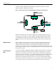
crossbar switch are distributed so that the data is stored closest to where it enters the
application-specific integrated circuit (ASIC).
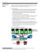
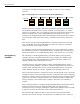
Figure 5. The F8 crossbar switch uses distributed buffers and multiple read and write ports.
With the F8 crossbar switch, the request is logged into the appropriate buffer, and then
each request is processed in a fair-share algorithm. The distributed buffer design and the
increased buffer sizes reduce the amount of arbitration and the number of retry cycles
required when processors request information, allowing the processors to do more useful
work.
Multiport Design
The F8 crossbar switch contains four write ports and thirteen read ports (Figure 5) and
allows simultaneous data transfer on any of those ports. By comparison, the Profusion
chipset has five read ports and five write ports. Despite having fewer write ports than
Profusion chipset, the F8 crossbar switch significantly improves performance because its port
to main memory is extremely wide, with a bandwidth more than five times greater than that
of the Profusion chipset.
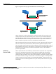
Cache Coherency
Filter
One of the challenges of designing an efficient multiprocessing architecture is to maintain a
consistent view of memory by all the processors and the I/O subsystem. This is typically
referred to as maintaining cache coherency. Because data is shared among several level
two (L2) caches on the processors, it is possible that data referred to by two different caches
could be inconsistent. In a multiprocessing server with dual processor buses, a memory
transaction from one processor bus has to look at, or snoop, the remote processor bus to
make sure that only the most recent data is in use. Every snoop cycle consumes bandwidth
on the remote processor bus and diminishes the performance of the system (Figure 6).
I/O Buffer
Processor Buffer
Memory Buffer
Write Port
3.2 GB/s
8.5 GB/s
Memory Network Interface
3.2 GB/s
3.2 GB/s
Read Ports
Left Processor Bus
Right Processor Bus
I/O Interface
Processor Buffer
I/O Buffer
Processor BufferProcessor Buffer
Memory Buffer
Write Port
3.2 GB/s
8.5 GB/s
Memory Network Interface
3.2 GB/s
3.2 GB/s
Read Ports
Left Processor Bus
Right Processor Bus
I/O Interface
Processor BufferProcessor Buffer