
HP F8 Architecture Technology Brief
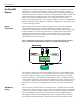

HP F8 Architecture
4
Overview of F8
Chipset
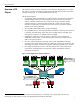
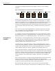
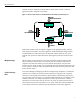
The backbone of the new 8-way architecture is the F8 chipset designed by HP. It includes
five memory controllers with patent-pending HP Hot-Plug RAID Memory and a multiported
crossbar switch (Figure 2). Product implementations will vary.
The F8 chipset supports:
• An aggregate memory bandwidth of 8.5 GB/s using five separate memory controllers
with 400 mega transfers per second
3
(MT/s) point-to-point connections. The RAID
memory controllers interface with the crossbar switch using a 200-MHz, double-
pumped connection to achieve the effective 400 MT/s. Each of the five memory
controllers has dual paths into channels of PC100 or PC133 synchronous dynamic
random access memory (SDRAM).
• Up to 64 GB of addressable memory using 2-GB DIMMs.
• Hot -plug RAID Memory, allowing replacement and addition of memory while the server
is operating. The RAID design stripes data across multiple memory cartridges while
storing parity information in a separate memory cartridge.
• Independent, nonblocking access to memory, processors, and I/O through the
multiported crossbar switch. A cache coherency filter reduces the amount of snoop
traffic on the processor buses.
• Up to four industry-standard PCI-X bridges, each with an embedded PCI Hot Plug
controller. Each of these bridges resides on a 400 MT/s, point-to-point connection, and
each bridge can support two PCI-X bus segments operating at speeds up to 100 MHz.
• Up to eight Intel Xeon MP processors. The Xeon MP processor is the multiprocessor
version of the seventh-generation IA-32 processor family, designed for high-end
workstations and servers.
Figure 2. Block diagram of the F8 chipset architecture
F8 Crossbar
Switch
Processors Processors
PCI-X
PCI-X
F8 Dual
Memory
Controller
F8 Dual
Memory
Controller
F8 Cache
Coherency
Filter
F8 Dual
Memory
Controller
F8 Dual
Memory
Controller
F8 Dual
Memory
Controller
F8 Dual
Memory
Controller
F8 Dual
Memory
Controller
F8 Dual
Memory
Controller
F8 Dual
Memory
Controller
F8 Dual
Memory
Controller
PCI-X
PCI-X
3.2GB/s, 400 MT/s
F8 Crossbar
Switch
3.2GB/s, 400 MT/s
ProcessorsProcessors
400 MT/s
400 MT/s
ProcessorsProcessors
-X
-X
F8 Dual
Memory
Controller
F8 Dual
Memory
Controller
F8 Dual
Memory
Controller
F8 Dual
Memory
Controller
F8 Cache
Coherency
Filter
F8 Dual
Memory
Controller
F8 Dual
Memory
Controller
F8 Dual
Memory
Controller
F8 Dual
Memory
Controller
F8 Dual
Memory
Controller
F8 Dual
Memory
Controller
F8 Dual
Memory
Controller
F8 Dual
Memory
Controller
F8 Dual
Memory
Controller
F8 Dual
Memory
Controller
F8 Dual
Memory
Controller
F8 Dual
Memory
Controller
F8 Dual
Memory
Controller
F8 Dual
Memory
Controller
F8 Dual
Memory
Controller
F8 Dual
Memory
Controller
PCI-X
PCI
64-bit, 100-MHz
PCI-X Hot Plug
133-MHz
SDRAM
Aggregate
I/O Bandwidth 3.2 GB/s
PCI-X PCI-XPCI-X PCI-X
Aggregate Memory
Bandwidth 8.5 GB/s
3
Bus speeds are described in mega transfers per second (MT/s). For example, a bus operating at 100 MHz and
transferring four data packets on each clock (quad-pumped) would have 400 MT/s.