
Instruction Manual

MAN0810-10-EN Specifications / Installation
__________________________________________________________________________________________________________________________________________________________________
12/18/2008 Page 3 of 4 ECN # 947
4.2 External DIP Switch Settings (or Jumpers Settings)
4.3 Wiring Examples
Note: The wiring examples show Positive Logic input wiring.
J1
Orange
Name
I1 IN1
I2 IN2
I3 IN3
I4 IN4
I5 IN5
I6 IN6
I7 IN7
I8 IN8
H1
HSC1 /
IN9
H2
HSC2 /
IN10
H3
HSC3 /
IN11
H4
HSC4 /
IN12
NC
No
Connect
NC
No
Connect
0V Ground
J3
Orange
Name
T1+
T/C / RTD IN1+ /
100 mV+
T1-
T/C / RTD IN1- /
100 mV-
T2+
T/C / RTD IN2+ /
100 mV+
T2-
T/C / RTD IN2- /
100 mV-
AQ1
10 V / 20 mA
OUT1
AQ2
0 V / 20 mA
OUT2
0V Ground
MA1 20 mA IN1
V1 10 V IN1
0V Ground
MA2 20 mA IN2
V2 10 V IN2
0V Ground
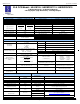
5 I/O Register Map
Registers
Description
%I1 to %I24 Digital Inputs
%I32 Output Fault
%I25 to %I31 Reserved
%Q1 to %Q16 Digital outputs
%Q17 Clear HSC1 accumulator to 0
%Q18
Totalizer: Clear HSC2
Quadrature 1-2: Accumulator 1
Reset to max – 1
%Q19 Clear HSC3 Accumulator to 0
%Q20
Totalizer: Clear HSC4
Quadrature 3-4: Accumulator 3
Reset to max – 1
%Q21 to %Q32 Reserved
%AI1 to %AI4 Analog inputs
%AI5, %AI6 HSC1 Accumulator
%AI7, %AI8 HSC2 Accumulator
%AI9, %AI10 HSC3 Accumulator
%AI11, %AI12 HSC4 Accumulator
%AQ1, %AQ2 PWM1 Duty Cycle
%AQ3, %AQ4 PWM2 Duty Cycle
%AQ5, %AQ6 PWM Prescale
%AQ7, %AQ8 PWM Period
%AQ9 to %AQ14 Analog outputs
Note: Not all XLe units contain the I/O listed in this table.
Registers PWM HSC Stepper
%AQ1
Start
Frequency
%AQ2
PWM1 Duty
Cycle
(32 bit)
HSC1
Preset
Value
Run
Frequency
%AQ3
%AQ4
PWM2 Duty
Cycle
(32 bit)
HSC2
Preset
Value
Accel Count
(32 bit)
%AQ5
%AQ6
PWM Prescale
(32 bit)
Run Count
(32 bit)
%AQ7
%AQ8
PWM Period
(32 bit)
Decel Count
(32 bit)
%Q1 Run
%I30 Ready/Done
%I31
Error
6 MJ2 Pinouts in Full and Half Duplex Modes
J2
Black
Name
0V Ground
V+* V+*
NC
No
Connect
Q12 OUT12
Q11 OUT11
Q10 OUT10
Q9 OUT9
Q8 OUT8
Q7 OUT7
Q6 OUT6
Q5 OUT5
Q4 OUT4
Q3 OUT3
Q2
OUT2 /
PWM2
Q1
OUT1 /
PWM1
V+* Supply for
Sourcing Outputs
I1
I2
I3
I4
H2
H3
H4
0V
I5
I6
I7
I8
NC
NC
H1
001XLE007
12-24
VDC
J1 Orange
Positive Logic
Digital In
Q1
Q2
Q3
Q4
Q9
Q10
Q11
Q12
Q5
Q6
Q7
Q8
V+
0V
LOAD
LOAD
LOAD
LOAD
LOAD
LOAD
LOAD
LOAD
LOAD
LOAD
LOAD
LOAD
10 - 30VDC
NC
001XLE00
8
J2 Black
Positive Logic
Digital Outputs
J3 Orange
Analog In / Analog Out
Note: A total of 2 Analog Inputs can be used (T/C, RTD, mV, mA,
and V).
0 -10 V Analog Out
AQ1
0V
10VDC
4 - 20 mA Analog Out
AQ1
0V
20mA
Thermocouple In
T1+
T1-
Some XLes have jumpers to set RS-
485 port termination, though most
use DIP Switches.
The External Jumpers or DIP
Switches are used for termination o
f
the RS-485 ports. The XLE is
shipped un-terminated.
To terminate, select one of the
j
umpers shipped with the product and
insert it based upon the option that is
desired or, select the switch and
configure based upon the option that
is desired.
DIPSW3: FACTORY USE
ONLY (tiny bootloader
firmware downloading).
NOT TO BE USED FOR
NORMAL OCS
OPERATION.
DIPSW2: MJ2 Termination
(Default – none)
DIPSW1: MJ1 Termination
(Default – none)
001XLE037
A
s seen when looking at the top of the XLE unit: Refer to Section
3 for the location of the External Jumpers.
0 – 10 V Analog In
0-10VDC
MA1
V1
0V
NC
RTD In
T1+
T1-
0V
mV In
T1+
T1-
0V
100mV+
100mV-
Note: Be sure to
wire 0 V to V1 as
shown for proper
operation.
Note: Loop Power (LOOP
PWR) requirements are
determined by the transmitter
specification.
LOOP PWR
20mA
MA1
V1
0V
20 mA Analog In
001XLE037-R1
DIPSW3: FACTORY USE
ONLY (tiny bootloader
firmware downloading).
NOT TO BE USED FOR
NORMAL OCS
OPERATION.
DIPSW2: MJ2 Termination
(Default – none)
DIPSW1: MJ1 Termination
(Default – none)
Full Duplex
Half Duplex
Pin MJ2 Pins
Signal Direction
8
TXD OUT
7
RXD IN
6
0 V Ground
5*
+5 60mA OUT
4
TX- OUT
3
TX+ OUT
2
RX- IN
1
RX+ IN
1
8
* +5Vdc 60mA Max on XLe Rev E and later
Pin MJ2 Pins
Signal Direction
8
TXD OUT
7
RXD IN
6
0 V Ground
5*
+5 60mA OUT
4
TX- OUT
3
TX+ OUT
2
TX-/RX- IN/OUT
1
TX+/RX+ IN/OUT
1
8