
User's Manual


7
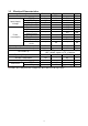
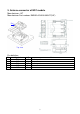
4. Interface of Connector of NFC module
Manufacturer: JST
Manufacturer Part number: 11FHSY-RSM1-GAN-TB(HF)
Pin definition
Pin
Symbol I/O Note
1
VBAT I Power supply from battery (2.8V - 5.5V)
2
VDDIO I Power supply to I/O (1.62V – 3.6V)
3
I
2
C -SDA I/O BSC Serial Data Line, active low
4
I
2
C -SCL I BSC Serial Clock
5
GND G Ground
6
IRQ-NFC O BSC request, active high (Host_Wake)
7
NFC_PRESENCE
G Ground
8
REG_UP I NFC Power-on
9
VDD_Ext_SE O
Power supply to External Secure Element
(1.8V or 3.0V)
10
UIM_PWR I Power supply to UICC (1.78V – 3.3V)
11
SWP I/O SWP I/O 0 (Single-Wire Protocol interface)
S1
GND G Ground
S2
GND G Ground
Remark: The connector is bottom conduct with golden plating of FPC
cable
Pin 1
Pin 1