
User's Manual
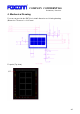


COMPANY CONFIDENTIAL
Preliminary Datasheet
24
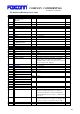
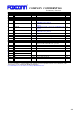
49 SDIO DATA1 I/O 4 lines for SDIO data exchange 1.8V
50 SDIO DATA0 I/O 4 lines for SDIO data exchange 1.8V
51 SDIO CMD I/O SDIO Command Interface 1.8V
52 SDIO CLK I SDIO 3.0 Clock 1.8V
53 UART WAKE O Bluetooth host Wake. Active Low 3.3V
54 UART CTS I UART Clear To Send, Active low, connected to
UART RTS on the platform.
1.8V
55 UART TX O UART Transmit Data, connected to UART RX on the
platform.
1.8V
56 UART RX I UART Receive Data, connected to UART TX on the
platform.
1.8V
58 UART RTS O UART Request To Send, Active low, connected to
UART CTS on the platform.
1.8V
58 PCM FR1 I/O PCM Synchronous data sync/ I2S Word Select 1.8V
59 PCMIN I PCM Synchronous data input/ I2S Serial Data IN 1.8V
60 PCMOUT O PCM Synchronous data output/ I2S Serial Data OUT
1.8V
61 PCMCLK I/O PCM Clock/ I2S Continuous Serial Clock (SCK) 1.8V
62 GND GND Ground
63 W_DISABLE#2 I Active low, debounced signal when applied by the
platform it will disable BT radio operation
3.3V
64 LED#2 - No connection -
65 LED#1 - No connection -
66-67 Reserved - Reserved LGA pin
68 GND GND Ground
69
*(a)
USB_D-
70
*(a)
USB _D+
- No connection -
71 GND GND Ground
72-73 3.3V Power Power voltage input pin 3.3V
74-76,
others
GND GND Ground
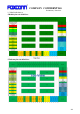
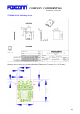
The pin-out definition is following NGFF1216 standard, but removed partial functions such as PCIE, BT_USB.
All of function used is following the BCM4324 application.
*(a) FOXCONN remove the function according to BCM4324 function.