
User's Manual
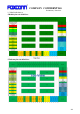
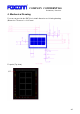
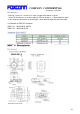


COMPANY CONFIDENTIAL
Preliminary Datasheet
23
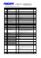
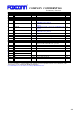
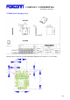
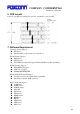
- Pin definition (Module point of view):
Pin No.
Pin Name Type Description Voltage
1-3 UIM_power_in/GPIO1
UIM_power_out
UIM_SWP
I/O No connection -
4-5 3.3V Power Power voltage input pin 3.3V
6 GND GND Ground -
7 Reserved I/O Reserved LGA pin -
8
*(a)
ALERT - No connection -
9
*(a)
I2C CLK - No connection -
10
*(a)
I2C DATA - No connection -
11
*(a)
COEX1 - No connection -
12
*(a)
COEX2 - No connection -
13
*(a)
COEX3 - No connection -
14-15 SYSCLK/GNSS0
TX_Blanking/GNSS1
- Reserved LGA pin, No connection
16 Reserved I/O Reserved LGA pin, No connection
17 GND GND Ground
18-19 Reserved - Reserved LGA pin, No connection
20 GND GND Ground
21-22 Reserved - Reserved LGA pin, No connection
23 GND GND Ground
24-25 Reserved - Reserved LGA pin, No connection
26 GND GND Ground
27 SUSCLK (32KHz) I 32.768 kHz clock supply input that is provided by
PCH to reduce power and cost for the module.
SUSCLK will have a duty cycle that can be as low as
30% or as high as 70%. 200ppm.
3.3V
28 W_DISABLE#1 I No connection
29
*(a)
PEWAKE# - No connection -
30
*(a)
CLKREQ# - No connection -
31
*(a)
PERST# - No connection -
32 GND GND Ground
33
*(a)
REFCLKN0
34
*(a)
REFCLKP0
- No connection -
35 GND GND Ground
36
*(a)
PETn0
37
*(a)
PETp0
- No connection -
38 GND GND Ground
39
*(a)
PERn0
40
*(a)
PERp0
- No connection -
41 GND GND Ground
42-44 Reserved - Reserved LGA pin, No connection
45 SDIO Reset I
SDIO sideband GPIO pin to enable/disable (reset) the
WiFi function. Platform firmware is required to
assert/de-assert this pin on every boot (warm and
cold). The WiFi device may use 0.5 to 1 mW in reset,
Active Low
1.8V
46 SDIO Wake O SDIO Host Wake. Note in band SDIO wake is not
used for non-active modes, Active Low. Require pull
up on the host side ( recommended 15K to 100K )
1.8V
47 SDIO DATA3 I/O 4 lines for SDIO data exchange 1.8V
48 SDIO DATA2 I/O 4 lines for SDIO data exchange 1.8V