
User's Manual
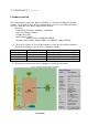
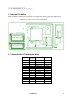
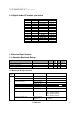
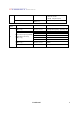
Table Of Contents

Confidential
5
2.2 Digital Audio I/F module pin define
Pin NO. Pin Type
Description Remark
1 - Ground B_J3
2 I BT_RST B_J3
3 Power BT_VDD33 B_J3
4 I
URT_CTS B_J3
5 O
URT_RTS B_J3
6 I
URT_RX B_J3
7 O
URT_TX B_J3
8 O
MUTE B_J3
9 -
Ground B_J3
10 -
Ground B_J3
11 O
PCM_SYNC B_J3
12 O
PCM_CLK B_J3
13 O
PCM_OUT B_J3
14 - Ground B_J3
3. Electrical Specification
3.1 Absolute Maximum Rating
Symbol Condition Min. Typ.
Max
.
Unit
VDD33 VDD33 Respect to GND 3.0 3.3 3.6 V
Operating Temperature -- -10 25 70
℃
Storage Temperature -- -40 25 85
℃
3.2 Bluetooth RF Specification
Test
station
Test item Test Condition Test Spec and Comments
Program Customer Specific FW N/A Pass
Write BD Address N/A Pass
Standby 0.0005~0.005A
Current Consumption
Max Consumption
(Continuous Tx )
0.036~0.054A
Output power test(class 2) Channel 0, 39, 78
-2dBm
≤
Output Power
≤
+3.0dBm
Power control Channel 39 2dBm<∆<8dBm
Initial Carrier Frequency Tolerance
Test
Channel 39 -25KHz<∆<25KHz
Carrier Frequency Drift Test Channel 78 Drift Rate/50us: -20KHz<∆<20KHz
DH1: -25KHz<∆<25KHz
DH3: -40KHz<∆<40KHz
DH5: -40KHz<∆<40KHz
PT
Multi-slot Sensitivity Test Channel 0,39,78
(BER<0.1%)
≤
-84dBm
+1.66
1.66dBm