
User Manual


11/04/08
16
PD-60357
IR3802AMPbF
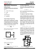
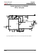
Programming the Current-Limit
The Current-Limit threshold can be set by
connecting a resistor (R
SET
) from drain of the
low-side MOSFET to the OCSet pin. The
resistor can be calculated by using equation (3).
The R
DS(on)
has a positive temperature
coefficient and it should be considered for the
worse case operation. This resistor must be
placed close to the IC, place a small ceramic
capacitor from this pin to power ground (PGnd)
for noise rejection purposes.
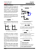
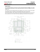
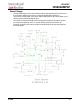
Layout Consideration
The layout is very important when designing high
frequency switching converters. Layout will affect
noise pickup and can cause a good design to
perform with less than expected results.
Start to place the power components, making all
the connection in the top layer with wide, copper
filled areas.
The inductor, output capacitor and the IR3802A
should be as close to each other as possible.
This helps to reduce the EMI radiated by the
power traces due to the high switching currents
through them. Place the input capacitor directly to
the Vin pin of IR3802A. To reduce the ESR
replace the single input capacitor with two
parallel units.
The feedback part of the system should be kept
away from the inductor and other noise sources.
The critical bypass components such as
capacitors for Vcc and Vc should be close to their
respective pins. It is important to place the
feedback components including feedback
resistors and compensation components close to
Fb and Comp pins.
In a multilayer PCB use one layer as a power
ground plane and have a control circuit ground
(analog ground), to which all signals are
referenced. The goal is to localize the high
current path to a separate loop that does not
interfere with the more sensitive analog control
function. These two grounds must be connected
together on the PC board layout at a single point.
The Power QFN is a thermally enhanced
package. Based on thermal performance it is
recommended to use at least a 4-layers PCB. To
effectively remove heat from the device the
exposed pad should be connected to the ground
plane using vias.
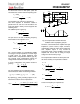
-(3)-
R
IR
=I=I
DS(on)
OCSetOCSet
)L(criticalSET
∗
13.7KΩ=R=R
10.1A=A1.11.5)*(6AI
F*L*V
V
*)VV(i
current ripple Inductor:i
Current Output Max:I
:where
2
i
)5.1*(II
V for usedis 5V if
MOSFET side-low for mΩ 24 Use :Note
27mΩ=.51* 18mΩ=R
7OCSet
SET
sin
o
oin
o
oSET
cc
DS(on)
+=
=Δ
Δ
Δ
+=
-