
User Manual


11/04/08
15
PD-60357
IR3802AMPbF
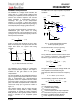
Based on the frequency of the zero generated by
output capacitor and its ESR versus crossover
frequency, the compensation type can be
different. The table below shows the
compensation types and location of crossover
frequency.
Select crossover frequency:
Fo=60kHz
Since: FLC<Fo<Fs/2<FESR, typeIII method B is
selected to place the poles and zeros.
The following design rules will give a crossover
frequency approximately one-tenth of the
switching frequency. The higher the band width,
the potentially faster the load transient response.
The DC gain will be large enough to provide high
DC-regulation accuracy (typically -5dB to -12dB).
The phase margin should be greater than 45
o
for
overall stability.
Desired Phase Boost:
Ceramic
F
LC
<F
o
<F
s/2
<F
ESR
Type III(PID)
Method B
Tantalum,
ceramic
F
LC
<F
o
<F
ESR
<F
s/2
Type III(PID)
Method A
Electrolytic
, Tantalum
F
LC
<F
ESR
<F
o
<F
s/2
Type II(PI)
Output
capacitor
F
ESR
vs. F
o
Compensator
type
Ω=Ω==
Ω=Ω==
Ω=
Ω==
===
===
Ω=
=
=
==
=
Θ
Θ+
=
=
Θ+
Θ
=
K2.40R :Select ,K30.40R ;R*
VV
V
R
K6.80R:Select ,K97.80R ;R
F*C*2
1
R
K61.2R :Select
g
1
R check ,K
60.2R ;
F*C*2
1
R
:R and R ,R Calculate
pF22C :Select ,pF8.30C ;
R*F*2
1
C
nF0.1C :Select 0.86nF,C ;
R*F*2
1
C
:C and C Calculate
34.8KR :Select
g
2
R check ,KΩ56.34=R ,
V*C
V*
C*L*F*2
R
180pFC :Select
F*0.5F and F*5.0F :Select
kHz28.340F
Sin1
Sin1
*FF
kHz58.10F
Sin1
Sin1
*FF
998
refo
ref
9
8810
2Z7
8
10
m
1010
2P7
10
9810
33
33P
3
44
3
Z1
4
34
3
m
33
in7
OSCooo
3
7
sP32ZZ1
2P
o2P
2Z
o2Z
-
≥
≥
-
-
π
π
π
π
π
o
max
70Θ =
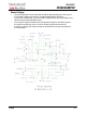
Table1- The compensation type and location
of F
ESR
versus F
o
The details of these compensation types are
discussed in application note AN-1043 which can
be downloaded from IR’s website at www.irf.com.
For this design we have:
V
in
=12V
V
o
=1.8V
V
osc
=1.25V
V
ref
=0.6V
g
m
=1000umoh
L
o
=2.2uH
C
o
=6x22uF, ESR=0.5mOhm
F
s
=300kHz
The value of the capacitance used in the
compensator design must be the small signal
value. For instance, the small signal capacitance
of the 22uF capacitor used in this design is 12uF
at 1.8 VDC bias and 600 kHz frequency. It is this
value that must be used for all computations
related to the compensation. The small signal
value may be obtained from the manufacturer’s
datasheets, design tools or SPICE models.
Alternatively, they may also be inferred from
measuring the power stage transfer function of
the converter and measuring the double pole
frequency
FLC and using equation (11) to
compute the small signal
Co.
These result to:
F
LC
=12.65kHz
F
ESR
=4.4MHz
F
s/2
=150kHz
(
)
soESRo
F1/10~1/5F and FF *
≤
<