
User Manual


11/04/08
11
PD-60357
IR3802AMPbF
Application Information
Design Example:
The following example is a typical application for
the IR3802A. The application circuit is shown in
page 17.
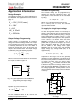
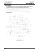
Output Voltage Programming
Output voltage is programmed by reference
voltage and external voltage divider. The Fb pin
is the inverting input of the error amplifier, which
is internally referenced to 0.6V. The divider is
ratioed to provide 0.6V at the Fb pin when the
output is at its desired value. The output voltage
is defined by using the following equation:
When an external resistor divider is connected to
the output as shown in figure 10.
Equation (4) can be rewritten as:
For the calculated values of R
8
and R
9
see
feedback compensation section.
kHz300F
mV30ΔV
A6I
V8.1V
)maxV,2.13V,(12V
s
o
o
o
in
=
=
=
=
≤
)4 --(
R
R
1VV
9
8
refo
⎟
⎟
⎠
⎞
⎜
⎜
⎝
⎛
+∗=
Fig. 10: Typical application of the IR3802A for
programming the output voltage
)5 --(
VV
V
RR
refO
ref
89
⎟
⎟
⎠
⎞
⎜
⎜
⎝
⎛
−
∗=
Soft-Start Programming
The soft-start timing can be programmed by
selecting the soft-start capacitance value. The
start-up time of the converter can be calculated
by using:
Where T
start
is the desired start-up time (ms)
For a start-up time of 11ms, the soft-start
capacitor will be 0.22uF.
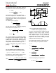
Vc supply for single input voltage
To drive the high-side switch, it is necessary to
supply a gate voltage at least 4V greater than the
bus voltage. This is achieved by using a charge
pump configuration as shown in figure 11. This
method is simple and inexpensive. The operation
of the circuit is as follows: when the lower
MOSFET is turned on, the capacitor (C1) is
pulled down to ground and charges, up to V
BUS
value, through the diode (D1). The bus voltage
will be added to this voltage when upper
MOSFET turns on in next cycle, and providing
supply voltage (Vc) through diode (D2). Vc is
approximately:
Capacitors in the range of 0.1uF are generally
adequate for most applications. The diodes must
be a fast recovery device to minimize the amount
of charge fed back from the charge pump
capacitor into V
BUS
. The diodes need to be able
to block the full power rail voltage, which is seen
when the high side MOSFET is switched on. For
low voltage application, schottky diodes can be
used to minimize forward drop across the diodes
at start up.
Fig. 11: Charge pump circuit to generate
Vc voltage
(
)
)6 --(VVV2V
2D1DbusC
+
−
∗
≅
)1 --(TA20C
startSS
*
μ
≅
Fb
IR3624
V
OUT
R
9
R
8
IR3802A