
PCI/CardBus Modem Designer's Guide RCV56HCF

RCV56HCF PCI/CardBus Modem Designer’s Guide
1129
ROCKWELL PROPRIETARY INFORMATION
3-9
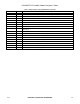
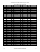
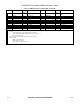
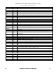
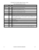
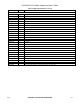
Table 3-2. Bus Interface Pin Signal Definitions (Cont’d)
Label I/O Type Signal Name/Description
MDP INTERFACE
DA0-DA4 Ot2
Device Bus Address Lines 0-4.
Connect to the MDP RS0-RA4 pins, respectively.
DD0-DD7 It/Ot12
Device Bus Data Line 0-7.
Connect to the MDP D0-D7 pins, respectively.
DRD# Ot2
Device Bus Read Enable.
Connect to the MDP READ# pin.
DWR# Ot2
Device Bus Write Enable.
Connect to the MDP WRITE# pin.
DRESET# Ot2
External Device Active Low Reset.
Connect to the MDP RESET1# and RESET2# pins.
WKRES# Ot12
Wakeup Reset.
Active low wake input.
Connect to the MDP WKRES# pin.
MODEM_CS# Ot2
MDP Data Pump Chip Select.
MODEM_CS# output low selects the MDP. Connect to the MDP CS# pin.
MODEM_IRQ It
MDP Interrupt Request.
MODEM_IRQ is the active low interrupt request from the MDP. Connect to the
MDP IRQ pin.
MODEM_CLK Ot2
Modem Clock.
Output clock for MDP. Connect to MDP XTLI pin.
M_TXCLK It
Modem Transmit Clock.
Connect to MDP M_TXCLK pin.
M_TX Ot2
Modem Transmit Data.
Connect to MDP M_TX pin.
M_RXCLK It
Modem Receive Clock.
Connect to MDP M_RXCLK pin.
M_RX It
Modem Receive Data.
Connect to MDP M_RX pin.
SI_FRAME It/Ot
SI Frame.
8 kHz frame sync; rising edge starts frame. Connect to MDP SI_FRAME pin.
SI_CLK It/Ot
SI Clock.
Connect to MDP SI_CLK pin.
SI_DD It
SI Data Downstream.
Connect to MDP SI_DD pin.
SI_DU Ot2
SI Data Upstream.
Connect to MDP SI_DU pin.