RCV56HCF PCI/CardBus Modem Designer's Guide (Preliminary) ROCKWELL PROPRIETARY INFORMATION. DISSEMINATION OR USE OF THIS INFORMATION IS NOT PERMITTED WITHOUT THE WRITTEN PERMISSION OF ROCKWELL INTERNATIONAL. Order No. 1129 Rev.
RCV56HCF PCI/CardBus Modem Designer’s Guide NOTICE Information furnished by Rockwell International Corporation is believed to be accurate and reliable. However, no responsibility is assumed by Rockwell International for its use, nor any infringement of patents or other rights of third parties which may result from its use. No license is granted by implication or otherwise under any patent rights of Rockwell International other than for circuitry embodied in Rockwell products.
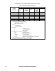
RCV56HCF PCI/CardBus Modem Designer’s Guide Table of Contents 1. INTRODUCTION .............................................................................................................................................1-1 1.1 SUMMARY.................................................................................................................................................1-1 1.2 FEATURES ...................................................................................................................
RCV56HCF PCI/CardBus Modem Designer’s Guide 2.13.1 Commanded Tests......................................................................................................... .................2-4 2.13.2 Power On Reset Tests ....................................................................................................................2-4 2.14 LOW POWER SLEEP MODE ...................................................................................................................2-4 3. HARDWARE INTERFACE.....
RCV56HCF PCI/CardBus Modem Designer’s Guide List of Figures Figure 1-1. RCV56HCF System Overview..........................................................................................................................1-4 Figure 1-2. RCV56HCF Hardware Configuration Block Diagram.........................................................................................1-5 Figure 1-3. Typical Audio Signal Interface (U.S.) .........................................................................................
RCV56HCF PCI/CardBus Modem Designer’s Guide List of Tables Table 1-1. Modem Models and Functions ..........................................................................................................................1-3 Table 1-2. Typical Signal Routing - Voice Mode ............................................................................................................... 1-11 Table 1-3. Relay Positions - VoiceView Mode ................................................................................
RCV56HCF PCI/CardBus Modem Designer’s Guide 1. INTRODUCTION 1.1 SUMMARY The Rockwell RCV56HCF-PCI Host-Controlled Modem Device Family supports high speed analog data, high speed fax, ISDN, DSVD, AudioSpan, speakerphone, audio/voice, and VoiceView operation. It operates with PSTN or ISDN telephone lines in the U.S. and world-wide and is offered in several device models (see Table 1-1).
RCV56HCF PCI/CardBus Modem Designer’s Guide • AudioSpan (simultaneous audio/voice and data)* − ITU-T V.61 modulation (4.8 kbps data plus audio) − Handset, headset, or half-duplex speakerphone • ITU-T V.70 DSVD (option) − ITU-T G.729 Annex A with interoperable G.
RCV56HCF PCI/CardBus Modem Designer’s Guide Table 1-1. Modem Models and Functions Supported Functions Marketing K56flex, V.34 Fax6 Voice/Audio/ VoiceView/ AudioSpan6 ISDN5,6 Full-duplex Speakerphone (FDSP) and DSVD W-Class Model Number1 RCV56HCF/ISDN Y Y Y Y – RCV56HCFW/ISDN Y Y Y Y Y RCV56HCF/SP Y Y – Y – RCV56HCFW/SP Y Y – Y Y RC56HCF Y – – – – RC56HCFW Y – – – Y Notes: 1.
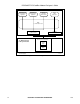
RCV56HCF PCI/CardBus Modem Designer’s Guide PC Software Win32-based communications application Win16-based communications application MS-DOS application (MS-DOS Box) Win32 NDIS application Win95 Communications Stack RC56HCF Serial Port Driver* Modem Hardware on Motherboard or Plug-in Module RC56HCF WAN Miniport Driver* RCV56HCF Modem Device Set Hardware Bus Interface (BIF)* Modem Data Pump (MDP)* * Rockwell supplied 1123F1 SO Figure 1-1.
RCV56HCF PCI/CardBus Modem Designer’s Guide RC56HCF MODEM DEVICE SET VOICE* DAA AND TELEPHONE HANDSET INTERFACE TXA TELEPHONE LINE RXA CID* OH HOST INTERFACE BUS INTERFACE (BIF) MODEM DATA PUMP (MDP) TELEPHONE HANDSET* RING * OPTIONAL USE (SUPPORTED BY MODEL HARDWARE AND SOFTWARE). a.
RCV56HCF PCI/CardBus Modem Designer’s Guide DAA AND TELEPHONE HANDSET INTERFACE RCV56HCF MODEM DEVICE SET TXA TELEPHONE LINE RXA CID* OH RING HOST INTERFACE BUS INTERFACE (BIF) MODEM DATA PUMP (MDP) DC FEED LCS* TELEPHONE HANDSET (OPTIONAL) VOICE* SPKR* MIC* AUDIO INTERFACE (OPTIONAL) ISDN U OR S/T INTERFACE SPEAKER* MICROPHONE* ISDN LINE * OPTIONAL USE (SUPPORTED BY MODEL HARDWARE AND SOFTWARE). c.
RCV56HCF PCI/CardBus Modem Designer’s Guide 1.3 TECHNICAL OVERVIEW 1.3.1 General Description The RCV56HCF Device Set provides the processing core for a complete system design featuring data/fax modem, DSVD, AudioSpan, speakerphone, voice/audio, and VoiceView depending on specific model (Table 1-1). Note: RCV56HCF Device Set refers to the family of single device modem models listed in Table 1-1. The modem is the full-featured, self-contained data modem/fax modem/DSVD/voice/audio/speakerphone solution.
RCV56HCF PCI/CardBus Modem Designer’s Guide Speakerphone Mode (ISDN and SP Models) The speakerphone mode features an advanced proprietary speakerphone algorithm which supports full-duplex voice conversation with both acoustic and line echo cancellation. Parameters are constantly adjusted to maintain stability with automatic fallback from full-duplex to pseudo-duplex operation. The speakerphone algorithm allows position independent placement of microphone and speaker.
RCV56HCF PCI/CardBus Modem Designer’s Guide 1.3.5.2 Serial EEPROM Interface A serial EEPROM is required to store the Maximum Latency, Minimum Grant, Device ID, Vendor ID, Subsystem ID, and Subsystem Vendor ID parameters for the PCI Configuration Space Header. The serial EEPROM interface connects to an Microchip 93LC66B, Atmel AT93C66, or equivalent 256 x 16 serial EEPROM.
RCV56HCF PCI/CardBus Modem Designer’s Guide LCS_L1# IRING_L1# VOICE# OH_L1# CID_L1# VC_L1 TXA1_L1 TXA2_L1 RXA_L1 HYBRD & XFRMR SSI & BRDGE CALLID RELAY SURG PROT OH RELAY TELOUT_L1 RCV56HCF MODEM DEVICE TELIN_L1 TEL LINE CUR SRC HANDSET HYBRID TEL HANDSET RNG DET VOICE RELAY LCS TELEPHONE LINE/TELEPHONE HANDSET INTERFACE CIRCUIT MIC_M MIC_V SPKROUT_M BIAS AMP/ SOUNDUCER (OPTIONAL) MICROPHONE HEADPHONE AUDIO/HEADPHONE INTERFACE CIRCUIT 1123F1-3 AIF 3R-US Figure 1-3.
RCV56HCF PCI/CardBus Modem Designer’s Guide Table 1-2. Typical Signal Routing - Voice Mode +VLS= Command Description Input Selected Output Selected VOICE# CID_L1# OH_L1# Output Output Output Activated Activated Activated 0 Modem on hook. Phone connected to Line . . No No Yes 1 Modem connected to Line.
RCV56HCF PCI/CardBus Modem Designer’s Guide This page is intentionally blank.
RCV56HCF PCI/CardBus Modem Designer’s Guide 2. TECHNICAL SPECIFICATIONS 2.1 ESTABLISHING DATA MODEM CONNECTIONS Dialing DTMF Dialing. DTMF dialing using DTMF tone pairs is supported in accordance with ITU-T Q.23. The transmit tone level complies with Bell Publication 47001. Pulse Dialing. Pulse dialing is supported in accordance with EIA/TIA-496-A. Blind Dialing. The modem can blind dial in the absence of a dial tone if enabled by the X0, X1, or X3 command.
RCV56HCF PCI/CardBus Modem Designer’s Guide Fall Forward/Fallback (K56flex, V.34/V.32 bis/V.32) During initial handshake, the modem will fallback to the optimal line connection within K56flex/V.34/V.32 bis/V.32 mode depending upon signal quality if automode is enabled by the +MS command. When connected in K56flex/V.34/V.32 bis/V.
RCV56HCF PCI/CardBus Modem Designer’s Guide 2.6.1 Online Voice Command Mode This mode results from the connection to the telephone line or a voice/audio I/O device (e.g., microphone, speaker, or handset) through the use of the +FCLASS=8 and +VLS commands. After mode entry, AT commands can be entered without aborting the connection. 2.6.
RCV56HCF PCI/CardBus Modem Designer’s Guide software control modem operation. Most VoiceView commands use an extended syntax starting with the characters "-S", which signifies the capability to switch between voice and data. 2.11 CALLER ID Caller ID can be enabled/disabled using the +VCID command. When enabled, caller ID information (date, time, caller code, and name) can be passed to the DTE in formatted or unformatted form.
RCV56HCF PCI/CardBus Modem Designer’s Guide 3. HARDWARE INTERFACE 3.1 HARDWARE SIGNAL PINS AND DEFINITIONS The RCV56HCF (PCI) functional interface signals are shown in Figure 3-1. The Bus Interface hardware interface signals are shown by major interface in Figure 3-2. The Bus Interface pin assignments for the 176-pin TQFP are shown Figure 3-3 and are listed Table 3-1. The Bus Interface hardware interface signals are defined in Table 3-2.
RCV56HCF PCI/CardBus Modem Designer’s Guide AD[31:0] CBE0# CBE1# CBE2# CBE3# PCICLK PCIRST# FRAME# IDSEL DEVSEL# IRDY# TRDY# PAR REQ# GNT# INTA# STOP# PERR# SERR# PCI BUS 28.
RCV56HCF PCI/CardBus Modem Designer’s Guide 27pF 5% 28.
VDD RESERVED RESERVED GND VDD RESERVED RESERVED RESERVED CARDBUS# SROMCS SROMIN SROMOUT SROMCLK RESERVED RESERVED ISDN_CS# ISDN_INT# GND NC NC NC NC NC INTA# PCIRST# VDD PCICLK GND GNT# REQ# CLKRUN# AD31 GND AD30 AD29 AD28 AD27 VDD GND AD26 AD25 AD24 ORING_H1 ORING_H2 RH_L1# RESERVED GND I/O0 I/O1 I/O2 I/O3 I/O4 RESERVED RESERVED RESERVED GND VDD RESERVED RESERVED RESERVED RESERVED RESERVED RESERVED RESERVED RESERVED RESERVED RESERVED RESERVED RESERVED M_RX MODEM_IRQ VGG1 VDD VOICE# MUTE_L1# OH_L1# CID_L
RCV56HCF PCI/CardBus Modem Designer’s Guide Table 3-1.
RCV56HCF PCI/CardBus Modem Designer’s Guide Table 3-1.
RCV56HCF PCI/CardBus Modem Designer’s Guide Table 3-2. Bus Interface Pin Signal Definitions Label I/O Type Signal Name/Description SYSTEM XIN, XOUT It Ot2 Crystal In and Crystal Out. Connect XIN and XOUT to a 28.224 MHz external crystal circuit. VDD PWR Digital Supply Voltage. Connect to 3.3V. GND GND Digital Ground. Connect to digital ground. CARDBUS# It CardBus Interface Select. Selects CardBus (low) or PCI Bus (high) drive strength. For PCI Bus, connect to VCC through 1K ohm.
RCV56HCF PCI/CardBus Modem Designer’s Guide Table 3-2. Bus Interface Pin Signal Definitions (Cont’d) Label I/O Type Signal Name/Description PCI BUS INTERFACE (CONTINUED) PERR# I/Opsts (s/t/s) Parity Error. PERR# is used for the reporting of data parity errors. SERR# Ood (o/d) System Error. SERR# is an open drain output asserted to report address parity errors, data parity errors on the Special Cycle command, or any other system error where the result will be catastrophic.
RCV56HCF PCI/CardBus Modem Designer’s Guide Table 3-2. Bus Interface Pin Signal Definitions (Cont’d) Label I/O Type Signal Name/Description MDP INTERFACE DA0-DA4 Ot2 Device Bus Address Lines 0-4. Connect to the MDP RS0-RA4 pins, respectively. DD0-DD7 It/Ot12 Device Bus Data Line 0-7. Connect to the MDP D0-D7 pins, respectively. DRD# Ot2 Device Bus Read Enable. Connect to the MDP READ# pin. DWR# Ot2 Device Bus Write Enable. Connect to the MDP WRITE# pin.
RCV56HCF PCI/CardBus Modem Designer’s Guide Table 3-2. Bus Interface Pin Signal Definitions (Cont’d) Label I/O Type Signal Name/Description ISDN INTERFACE (NON-ISDN MODELS) DA0-DA3 Ot2 Device Bus Address Lines 0-3. Connect to the MDP only DD0-DD7 It/Ot12 Device Bus Data Line 0-7. Connect to the MDP only DRD# Ot2 Read Enable. Connect to the MDP only DWR# Ot2 Write Enable. Connect to the MDP only ISDN_CS# Ot2 ISDN Chip Select. Leave open. ISDN_INT It ISDN Interrupt Request. Connect to GND.
RCV56HCF PCI/CardBus Modem Designer’s Guide 33 141 143 XTLI XTLO DRESET# 67 130 11 12 64 65 66 144 1 3 4 6 8 9 10 69 68 32 86 CS# IRQ RS0 RS1 RS2 RS3 RS4 D0 D1 D2 D3 D4 D5 D6 D7 READ# WRITE# RESET2# RESET1# WKRES# 72 WKRES# MODEM_CLK NC BIF VDD NC VAA GND AGND NC MODEM_CS# MODEM_IRQ DA0 DA1 DA2 DA3 DA4 DD0 DD1 DD2 DD3 DD4 DD5 DD6 DD7 DRD# DWR# SI_FRAME SI_CLK SI_DD SI_DU 97 98 100 99 SI_FRAME SI_CLK SI_DD SI_DU M_TX M_TXCLK M_RXCLK M_RX 77 76 71 111 M_TX M_TXCLK M_RXCLK M_RX 79 107
D1 RESERVED D2 D3 RESERVED D4 RESERVED D5 D6 D7 RS0 RS1 PLLVDD AGND NC NC NC AGND AGND TELIN_L1 AGNDV TELOUT_L1 AVAA SPKROUT_M TXA1_L1 TXA2_L1 VREF VC_L1 MIC_V RXA_L1 AGNDM RESET2# MIC_M MICBIAS RESERVED GND RESERVED RESERVED RESERVED RESERVED RESERVED RESERVED RESERVED SLEEPO RESERVED M_RX RESERVED GND RESERVED IOM_DU RESERVED 108 107 106 105 104 103 102 101 100 99 98 97 96 95 94 93 92 91 90 89 88 87 86 85 84 83 82 81 80 79 78 77 76 75 74 73 RESERVED VDD SR1IO NC SR2IO SA2CLK RESERVED RESERVED SI_DD SI
RCV56HCF PCI/CardBus Modem Designer’s Guide Table 3-3.
RCV56HCF PCI/CardBus Modem Designer’s Guide Table 3-3.
RCV56HCF PCI/CardBus Modem Designer’s Guide Table 3-4. MDP Pin Signal Definitions Label I/O Type Signal/Definition OVERHEAD SIGNALS XTLI I Crystal Int. Connect the BIF MODEMCLK pin through a 33 Ω resistor. XTLO O Crystal Out. Leave open. VDD, AVDD PWR Digital Power Supply. To +3.3V and digital circuits power supply filter. AVAA PWR Analog Power Supply. To +3.3V and analog circuits power supply filter. GND GND Digital Ground. Connect to digital ground. AGND GND Analog Ground.
RCV56HCF PCI/CardBus Modem Designer’s Guide Table 3-4. MDP Signal Definitions (Cont'd) Label I/O Type Signal Name/Description TELEPHONE LINE/TELEPHONE/AUDIO INTERFACE SIGNALS AND REFERENCE VOLTAGE TXA1_L1 TXA2_L1 O(DF) Transmit Analog 1 and 2. The TXA1_L1 and TXA2_L1 outputs are differential outputs 180 degrees out of phase with each other. Each output can drive a 300 Ω load. RXA_L1 I(DA) Receive Analog.
RCV56HCF PCI/CardBus Modem Designer’s Guide Table 3-4.
RCV56HCF PCI/CardBus Modem Designer’s Guide 3.2 ELECTRICAL,SWITCHING,AND ENVIRONMENTAL CHARACTERISTICS 3.2.1 Power and Maximum Ratings The current and power requirements are listed in Table 3-5. The absolute maximum ratings are listed in Table 3-6. Table 3-5. Current and Power Requirements Current Typical Current (mA) Mode Power Maximum Current (mA) Typical Power (mW) Maximum Power (mW) Bus Interface (11229) Notes fIN = 28.224 MHz Operating 145 186 479 670 Modem Data Pump (R6776) fIN = 28.
RCV56HCF PCI/CardBus Modem Designer’s Guide 3.2.2 PCI Bus Table 3-7 summarizes the PCI DC specifications for 3.3V signaling. Table 3-8 summarizes the PCI AC specifications for 3.3V signaling. Table 3-7. PCI Bus DC Specifications for 3.3V Signaling Symbol Vcc Parameter Condition Supply Voltage Min Max Units 3.0 3.6 V V Vih Input High Voltage 0.5Vcc Vcc +0.5 Vil Input Low Voltage -0.5 0.3Vcc Vipu Input Pull-up Voltage 0.
RCV56HCF PCI/CardBus Modem Designer’s Guide 3.2.3 MDP The MDP digital electrical characteristics for the hardware interface signals are listed in Table 3-9. The MDP analog electrical characteristics for the hardware interface signals are listed in Table 3-10. Table 3-9. MDP Digital Electrical Characteristics Parameter Input High Voltage Type IA Type IE Input High Current Type IB Input Low Voltage Type IA Type IE Input Low Current Input Leakage Current Output High Voltage Symbol V Min. Typ. Max. 2.
RCV56HCF PCI/CardBus Modem Designer’s Guide Table 3-10. Analog Electrical Characteristics Name Type Characteristic Value RXA_L1, TELIN_L1 I (DA) Input Impedance AC Input Voltage Range Reference Voltage > 70K Ω 1.1 VP-P** +2.5 VDC TXA1_L1 TXA2_L1 TELOUT_L1 O (DD) Minimum Load Maximum Capacitive Load Output Impedance AC Output Voltage Range Reference Voltage DC Offset Voltage 300 Ω 0 µF 10 Ω 2.2 VP-P +2.
RCV56HCF PCI/CardBus Modem Designer’s Guide 3.3 INTERFACE TIMING AND WAVEFORMS 3.3.1 PCI Bus Timing The PCI interface timing conforms to the PCI Local Bus Specification, Production Version, Revision 2.1, June 1, 1995. 3.3.2 Serial EEPROM Timing The serial EEPROM interface timing is listed in Table 3-11 and is shown in Figure 3-6. Table 3-11. Timing - Serial EEPROM Interface Symbol Parameter Min Typ.
RCV56HCF PCI/CardBus Modem Designer’s Guide 3.3.3 External Device Bus Timing The external Device Bus timing is listed in Table 3-12 and illustrated in Figure 3-7. Table 3-12. Timing - External Device Bus Interface Symbol Description Min. Typ. Max.
RCV56HCF PCI/CardBus Modem Designer’s Guide t AH t AS DA0 - DA4 t CSS t CSH ISDN_CS# t RW DRD# t RDH t RDA DD0-DD7 Read data valid a. Read t AH t AS DA0 - DA4 t CSS t CSH ISDN_CS# t WW DWR# t WDS DD0-DD7 t WDH Write data valid a. Write 1123F3-8 EB Figure 3-7.
RCV56HCF PCI/CardBus Modem Designer’s Guide 3.3.4 IOM-2 Interface The interface timing is listed in Table 3-13 and shown in Figure 3-8. Table 3-13. Timing - IOM-2 Interface Symbol Parameter Min Typ.
RCV56HCF PCI/CardBus Modem Designer’s Guide This page is intentionally blank.
RCV56HCF PCI/CardBus Modem Designer’s Guide 4. DESIGN CONSIDERATIONS Good engineering practices must be followed when designing a printed circuit board (PCB) containing the modem device. This is especially important considering the high data bit rate, high fax rate, record/play of analog speech and music audio, and full-duplex speakerphone operation. Suppression of noise is essential to the proper operation and performance of the modem and interfacing audio and DAA circuits.
RCV56HCF PCI/CardBus Modem Designer’s Guide 3. 4. 5. 6. 7. Once sections have been roughly defined, place the components starting with the connectors and jacks. a) Allow sufficient clearance around connectors and jacks for mating connectors and plugs. b) Allow sufficient clearance around components for power and ground traces. c) Allow sufficient clearance around sockets to allow the use of component extractors. First, place the mixed analog/digital components (e.g.
RCV56HCF PCI/CardBus Modem Designer’s Guide 10. Minimize the number of through-hole connections (feedthroughs/vias) on traces carrying high frequency signals. 11. Keep all signal traces away from crystal circuits. 12. Distribute high frequency signals continuously on a single trace rather than several traces radiating from one point. 13. Provide adequate clearance (e.g., 60 mil minimum) around feedthroughs in any internal planes in the DAA circuit. 14.
RCV56HCF PCI/CardBus Modem Designer’s Guide 4.1.5 Ground Planes 1. In a 2-layer design, provide digital and analog ground plane areas in all unused space around and under digital and analog circuit components (exclusive of the DAA), respective, on both sides of the board, and connect them such a manner as to avoid small islands.
RCV56HCF PCI/CardBus Modem Designer’s Guide 4.1.8 Telephone and Local Handset Interface 1. Place common mode chokes in series with Tip and Ring for each connector. 2. Decouple the telephone line cables at the telephone line jacks. Typically, use a combination of series inductors, common mode chokes, and shunt capacitors. Methods to decouple telephone lines are similar to decoupling power lines, however, telephone line decoupling may be more difficult and deserves additional attention.
RCV56HCF PCI/CardBus Modem Designer’s Guide Table 4-2. Crystal Specifications - Surface Mount Characteristic Value Rockwell Part No. 5333R02-020 Electrical Frequency Frequency Tolerance 28.224 MHz nom. ±50 ppm (C = 16.5 and 19.5 pF) L Frequency Stability vs. Temperature vs.
RCV56HCF PCI/CardBus Modem Designer’s Guide Table 4-3. Crystal Specifications - Through Hole Characteristic Value Rockwell Part No. 333R44-011 Electrical Frequency Frequency Tolerance 28.224 MHz nom. ±50 ppm (C = 16.5 and 19.5 pF) L Frequency Stability vs. Temperature vs.
RCV56HCF PCI/CardBus Modem Designer’s Guide 4.4 PACKAGE DIMENSIONS The package dimensions are shown in Figure 4-1 (144-pin TQFP) and Figure 4-2 (176-pin TQFP) . D D1 D2 PIN 1 REF D D1 D1 D2 e b DETAIL A Dim. A A1 D1 A2 D D1 0.15 0.05 1.4 REF 22.25 21.75 20.0 REF D2 A2 0.0630 MAX 0.0020 0.0059 0.0551 REF 0.8563 0.8760 0.7874 REF 17.5 REF L A Inches* Max. Min. Millimeters Max. Min. 1.6 MAX 0.6890 REF 0.0197 0.0295 L1 0.75 0.5 1.0 REF e 0.50 BSC 0.0197 BSC 0.0394 REF b 0.17 0.
RCV56HCF PCI/CardBus Modem Designer’s Guide Figure 4-2.
RCV56HCF PCI/CardBus Modem Designer’s Guide This page is intentionally blank.
RCV56HCF PCI/CardBus Modem Designer’s Guide 5. SOFTWARE INTERFACE 5.1 PCI Configuration Registers The PCI Configuration registers are located in the BIF. Table 5-1 identifies the configuration register contents that are supported in the BIF device: Table 5-1.
RCV56HCF PCI/CardBus Modem Designer’s Guide 5.1.3 Command Register The Command Register bits are described in Table 5-2. Table 5-2. Command Register Bit Description 0 Controls a device’s response to I/O Space accesses. A value of 0 disables the device response. A value of 1 allows the device to respond to I/O Space accesses. State after RST# is 0. 1 Controls a device’s response to Memory Space accesses. A value of 0 disables the device response.
RCV56HCF PCI/CardBus Modem Designer’s Guide 5.1.5 Revision ID Field Initial part hardwired to 00. 5.1.6 Class Code Field Hardwired to 0x078000 to indicate communications controller. 5.1.7 Latency Timer Register The Latency Timer register specifies, in units of PCI bus clocks, the value of the Latency Timer for this PCI bus master. This register has 5 read/write bits (MSBs) plus 3 bits of hardwired zero (LSBs).
RCV56HCF PCI/CardBus Modem Designer’s Guide 5.3 SERIAL EEPROM INTERFACE The serial EEPROM interface is used to load PCI configuration parameters and CIS information (required for Card Bus operation) after a reset occurs. The PCI configuration information to be loaded requires 10 bytes of data. The CIS information requires 384 bytes of data. The minimum serial EEPROM size is 512 bytes (4096 bits).
RCV56HCF PCI/CardBus Modem Designer’s Guide 6. COMMAND SET The commands for the different models are listed by functional use in Table 6-1and alphanumerically in Table 6-2. Table 6-1.
RCV56HCF PCI/CardBus Modem Designer’s Guide Table 5-1. Command Set Summary - Functional Use Sort (Cont’d) Configuration Command Description Data/Fax Data/Fax/Voice Data/Fax/Voice/ Data/Fax/Voice/ Speakerphone Speakerphone/ ISDN Data Compression +DS Data Compression X X X X +DR Data Compression Reporting X X X X %E Enable/Disable Line Quality Monitor and AutoRetrain X X X X %L Line Signal Level X X X X %Q Line Signal Quality X X X X +A8E V.8 and V.
RCV56HCF PCI/CardBus Modem Designer’s Guide Table 5-1.
RCV56HCF PCI/CardBus Modem Designer’s Guide Table 6-2.
RCV56HCF PCI/CardBus Modem Designer’s Guide Table 5-2.
RCV56HCF PCI/CardBus Modem Designer’s Guide Table 5-2.
NOTES (Inside Back Cover)
REGIONAL SALES OFFICES Headquarters Rockwell Semiconductor Systems 4311 Jamboree Road, P.O. Box C Newport Beach, CA 92658-8902 Phone: (714) 221-4600 Fax: (714) 221-6375 European Headquarters Rockwell Semiconductor Systems S.A.R.L. Les Taissounieres B1 Route des Dolines Sophia Antipolis Cedex 06905 Valbonne France Phone: (33) 93 00 33 35 Fax: (33) 93 00 33 03 For more information: Call 1-800-854-8099 International information: Call 1-714-833-6996 URL Address: http://www.nb.rockwell.