
Product Manual


XR1 Datasheet
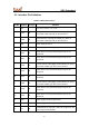
8
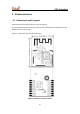
Pin No.
Symbol
I/O Type
Function
17
ADC
AI
ADC pin (See the following Note 2.)
18
GND
P
Power supply reference ground pin
Note:
1. P indicates power supply pins, I/O indicates input/output pins, and AI indicates analog
input pins.
2. This pin can only function as an ADC input and not a common I/O. If this pin is not
used, it must be disconnected. When this pin is used as an ADC input, the input
voltage range is 0 V to 2.5 V.
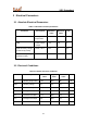
2.3 Test Pin Definition
Table 2-2 XR1 test pins
Note:
1 I/O indicates input/output pins.
2 During firmware burning, both PB02 and PB03 need to be connected to a low level.
When the module works properly, PB02 and PB03 cannot be connected to a low level
simultaneously.
3 Test pins are not recommended.
Pin No.
Symbol
I/O Type
Function
N/A
PB02
I/O
Connected to PB02 (pin 10) on the internal IC
N/A
PB03
I/O
Connected to PB03 (pin 11) on the internal IC