
Product Manual

WB3L Datasheet
Hangzhou Tuya Information Technology Co., Ltd. 8 V1.0.0
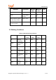
Note:
P indicates a power supply pin, I/O indicates an input/output pin, and AI indicates an
analog input pin.
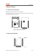
2.3 Test Pin Definition
Table 2-2 WB3L test pins
Pin No.
Symbol I/O Type
Function
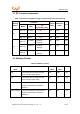
TP6 U2_RXD I/O UART2_RX, which is connected to the P1 pin on
the internal IC
TP2 F_SCK I/O Clock pin when data is downloaded from the flash
memory, which is connected to the P20 pin on the
internal IC
TP3 F_CSN I/O Command enabling pin when data is downloaded
from the flash memory, which is connected to the
P21 pin on the internal IC
TP4 F_SI I/O Data input pin when data is downloaded from the
flash memory, which is connected to the P22 pin on
the internal IC
TP5 F_SO I/O Data output pin when data is downloaded from the
flash memory, which is connected to the P23 pin on
the internal IC
Note:
Test pins are not recommended.
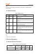
3. Electrical Parameters
3.1 Absolute Electrical Parameters
Table 3-1 Absolute electrical parameters
Parameter Description Minimum
Value
Maximum
Value
Unit
Ts Storage –40 105 °C