
Data Sheet
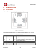


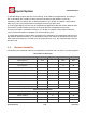


Table Of Contents
- 1.General Overview
- 1.1.Introduction
- 1.2.Features
- 1.3.Parameters
- 1.4.Ultra Low Power Technology
- 1.5.Major Applications
- 2.Hardware Overview
- 3.Pins and Definitions
- 3.1.GPIO
- 3.2.Secure Digital Input/Output Interface (SDIO)
- 3.3.Serial Peripheral Interface (SPI/HSPI)
- 3.4.Inter-integrated Circuit Interface (I2C)
- 3.5.I2S
- 3.6.Universal Asynchronous Receiver Transmitter (UART)
- 3.7.Pulse-Width Modulation (PWM)
- 3.8.IR Remote Control
- 3.9.ADC (Analog-to-digital Converter)
- 3.10.LED Light and Button
- 4.Firmware & Software Development Kit
- 5.Power Management
- 6.Clock Management
- 8.FCC Warming Statement
- This device complies with part 15 of the FCC Rules
- (1)This device may not cause harmful interference,
- (2)and this device must accept any interference re
- FCC Radiation Exposure Statement:
- This equipment complies with FCC radiation exposur
- Information to the user.
- Note: This equipment has been tested and found to
- -Reorient or relocate the receiving antenna.
- -Increase the separation between the equipment and
- -Connect the equipment into an outlet on a circuit
- -Consult the dealer or an experienced radio/TV tec
- 9.Appendix: QFN32 Package Size

ESP8266 Datasheet
Espressif Systems
Espressif Systems
June1,2015
11
/
32
6
TOUT
I
ADC Pin (note: an internal pin of the chip) can be used to
check the power voltage of VDD3P3 (Pin 3 and Pin4) or the
input voltage of TOUT (Pin 6). These two functions cannot be
used simultaneously.
7
CHIP_EN
I
Chip Enable.
High: On, chip works properly; Low: Off, small current
8
XPD_DCDC
I/O
Deep-Sleep Wakeup
;
GPIO16
9
MTMS
I/O
GPIO14; HSPI_CLK
10
MTDI
I/O
GPIO12; HSPI_MISO
11
VDDPST
P
Digital/IO Power Supply (1.8V~3.3V)
12
MTCK
I/O
GPIO13; HSPI_MOSI; UART0_CTS
13
MTDO
I/O
GPIO15; HSPI_CS; UART0_RTS
14
GPIO2
I/O
UART Tx during flash programming; GPIO2
15
GPIO0
I/O
GPIO0; SPI_CS2
16
GPIO4
I/O
GPIO4
17
VDDPST
P
Digital/IO Power Supply (1.8V~3.3V)
18
SDIO_DATA_2
I/O
Connect to SD_D2 (Series R: 200Ω); SPIHD; HSPIHD; GPIO9
19
SDIO_DATA_3
I/O
Connect to SD_D3 (Series R: 200Ω); SPIWP; HSPIWP; GPIO10
20
SDIO_CMD
I/O
Connect to SD_CMD (Series R: 200Ω); SPI_CS0; GPIO11
21
SDIO_CLK
I/O
Connect to SD_CLK (Series R: 200Ω); SPI_CLK; GPIO6
22
SDIO_DATA_0
I/O
Connect to SD_D0 (Series R: 200Ω); SPI_MSIO; GPIO7
23
SDIO_DATA_1
I/O
Connect to SD_D1 (Series R: 200Ω); SPI_MOSI; GPIO8
24
GPIO5
I/O
GPIO5
25
U0RXD
I/O
UART Rx during flash programming; GPIO3
26
U0TXD
I/O
UART Tx during flash progamming; GPIO1; SPI_CS1
27
XTAL_OUT
I/O
Connect to crystal oscillator output, can be used to provide BT
clock input
28
XTAL_IN
I/O
Connect to crystal oscillator input
29
VDDD
P
Analog Power 3.0V~3.6V
30
VDDA
P
Analog Power 3.0V~3.6V
31
RES12K
I
Serial connection with a 12 kΩ resistor and connect to the
ground
32
EXT_RSTB
I
External reset signal (Low voltage level: Active)