
Data Sheet


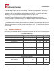


Table Of Contents
- 1.General Overview
- 1.1.Introduction
- 1.2.Features
- 1.3.Parameters
- 1.4.Ultra Low Power Technology
- 1.5.Major Applications
- 2.Hardware Overview
- 3.Pins and Definitions
- 3.1.GPIO
- 3.2.Secure Digital Input/Output Interface (SDIO)
- 3.3.Serial Peripheral Interface (SPI/HSPI)
- 3.4.Inter-integrated Circuit Interface (I2C)
- 3.5.I2S
- 3.6.Universal Asynchronous Receiver Transmitter (UART)
- 3.7.Pulse-Width Modulation (PWM)
- 3.8.IR Remote Control
- 3.9.ADC (Analog-to-digital Converter)
- 3.10.LED Light and Button
- 4.Firmware & Software Development Kit
- 5.Power Management
- 6.Clock Management
- 8.FCC Warming Statement
- This device complies with part 15 of the FCC Rules
- (1)This device may not cause harmful interference,
- (2)and this device must accept any interference re
- FCC Radiation Exposure Statement:
- This equipment complies with FCC radiation exposur
- Information to the user.
- Note: This equipment has been tested and found to
- -Reorient or relocate the receiving antenna.
- -Increase the separation between the equipment and
- -Connect the equipment into an outlet on a circuit
- -Consult the dealer or an experienced radio/TV tec
- 9.Appendix: QFN32 Package Size

ESP8266 Datasheet
Espressif Systems
Espressif Systems
June1,2015
10
/
32
2.
Hardware Overview
2.1.
Pin Definitions
The pin assignments for 32-pin QFN package is illustrated in Fig.2.
Figure 2 Pin Assignments
Table 2 below presents an overview on the general pin attributes and the functions of each pin.
Table 2 Pin Definitions
Pin
Name
Type
Function
1
VDDA
P
Analog Power 3.0 ~3.6V
2
LNA
I/O
RF Antenna Interface. Chip Output Impedance=50Ω
No matching required but we recommend that the π-type
matching network is retained.
3
VDD3P3
P
Amplifier Power 3.0~3.6V
4
VDD3P3
P
Amplifier Power 3.0~3.6V
5
VDD_RTC
P
NC (1.1V)