
Data Sheet
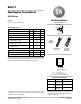

BC517
http://onsemi.com
2
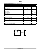
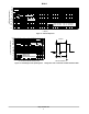
ELECTRICAL CHARACTERISTICS (T
A
= 25°C unless otherwise noted)
Characteristic Symbol Min Typ Max Unit
OFF CHARACTERISTICS
Collector−Emitter Breakdown Voltage
(I
C
= 2.0 mAdc, I
BE
= 0)
V
(BR)CES
30 − −
Vdc
Collector−Base Breakdown Voltage
(I
C
= 10 mAdc, I
E
= 0)
V
(BR)CBO
40 − −
Vdc
Emitter−Base Breakdown Voltage
(I
E
= 100 mAdc, I
C
= 0)
V
(BR)EBO
10 − −
Vdc
Collector Cutoff Current
(V
CE
= 30 Vdc)
I
CES
− − 500
nAdc
Collector Cutoff Current
(V
CB
= 30 Vdc, I
E
= 0)
I
CBO
− − 100
nAdc
Emitter Cutoff Current
(V
CB
= 10 Vdc, I
C
= 0)
I
EBO
− − 100
nAdc
ON CHARACTERISTICS (Note 1)
DC Current Gain
(I
C
= 20 mAdc, V
CE
= 2.0 Vdc)
h
FE
30,000 − −
−
Collector−Emitter Saturation Voltage
(I
C
= 100 mAdc, I
B
= 0.1 mAdc)
V
CE(sat)
− − 1.0
Vdc
Collector−Emitter Saturation Voltage
(I
C
= 10 mAdc, V
CE
= 5.0 Vdc)
V
BE(on)
− − 1.4
Vdc
SMALL−SIGNAL CHARACTERISTICS
Current−Gain − Bandwidth Product (Note 2)
(I
C
= 10 mAdc, V
CE
= 5.0 Vdc, f = 100 MHz)
f
T
− 200 −
MHz
1. Pulse Test: Pulse Width = 300 ms, Duty Cycle 2.0%.
2. f
T
= |h
fe
| • f
test
R
S
i
n
e
n
IDEAL
TRANSISTOR
Figure 1. Transistor Noise Model