
Data Sheet

© Semiconductor Components Industries, LLC, 2011
September, 2011 − Rev. 5
1 Publication Order Number:
BC517/D
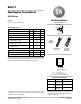
BC517
Darlington Transistors
NPN Silicon
Features
• These are Pb−Free Devices*
MAXIMUM RATINGS
Rating Symbol Value Unit
Collector−Emitter Voltage V
CES
30 Vdc
Collector−Base Voltage V
CB
40 Vdc
Emitter−Base Voltage V
EB
10 Vdc
Collector Current − Continuous I
C
1.0 Adc
Total Power Dissipation @ T
A
= 25°C
Derate above T
A
= 25°C
P
D
625
12
mW
mW/°C
Total Power Dissipation @ T
C
= 25°C
Derate above T
C
= 25°C
P
D
1.5
12
W
mW/°C
Operating and Storage Junction
Temperature Range
T
J
, T
stg
−55 to +150 °C
THERMAL CHARACTERISTICS
Characteristic Symbol Max Unit
Thermal Resistance, Junction−to−Ambient
R
q
JA
200 °C/W
Thermal Resistance, Junction−to−Case
R
q
JC
83.3 °C/W
Stresses exceeding Maximum Ratings may damage the device. Maximum
Ratings are stress ratings only. Functional operation above the Recommended
Operating Conditions is not implied. Extended exposure to stresses above the
Recommended Operating Conditions may affect device reliability.
*For additional information on our Pb−Free strategy and soldering details, please
download the ON Semiconductor Soldering and Mounting Techniques
Reference Manual, SOLDERRM/D.
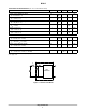
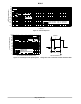
Device Package Shipping
†
ORDERING INFORMATION
BC517G TO−92
(Pb−Free)
5000 Units / Bulk
http://onsemi.com
BC517RL1G TO−92
(Pb−Free)
2000 / Tape & Reel
BC517ZL1G TO−92
(Pb−Free)
2000 / Ammo Pack
†For information on tape and reel specifications,
including part orientation and tape sizes, please
refer to our Tape and Reel Packaging Specifications
Brochure, BRD8011/D.
COLLECTOR 1
BASE
2
EMITTER 3
1
2
3
1
2
BENT LEAD
TAPE & REEL
AMMO PACK
STRAIGHT LEAD
BULK PACK
3
TO−92
CASE 29
STYLE 17
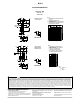
MARKING DIAGRAM
BC
517
AYWW G
G
A = Assembly Location
Y = Year
WW = Work Week
G = Pb−Free Package
(Note: Microdot may be in either location)