
Data Sheet
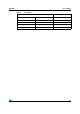
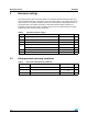
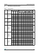
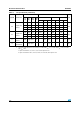

Table Of Contents

Maximum ratings HCF4093
4/13
2 Maximum ratings
Stressing the device above the rating listed in the “Absolute Maximum Ratings” table may
cause permanent damage to the device. These are stress ratings only and operation of the
device at these or any other conditions above those indicated in the Operating sections of
this specification is not implied. Exposure to Absolute Maximum Rating conditions for
extended periods may affect device reliability. Refer also to the STMicroelectronics SURE
Program and other relevant quality documents.
2.1 Recommended operating conditions
Table 4. Absolute maximum ratings
Symbol Parameter Value Unit
V
DD
Supply voltage -0.5 to + 22 V
V
I
DC Input voltage -0.5 to V
DD
+ 0.5 V
I
I
DC Input current ± 10 mA
P
D
Power dissipation per package 200 mW
Power dissipation per output transistor 100 mW
T
op
Operating temperature -55 to +125 °C
T
stg
Storage temperature -65 to +150 °C
Table 5. Recommended operating conditions
Symbol Parameter Value Unit
V
DD
Supply voltage 3 to 20 V
V
I
Input voltage 0 to V
DD
V
T
op
Operating temperature -55 to 125 °C