
Data Sheet
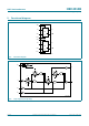

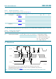
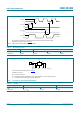

Table Of Contents
- 1. General description
- 2. Features and benefits
- 3. Applications
- 4. Ordering information
- 5. Functional diagram
- 6. Pinning information
- 7. Functional description
- 8. Limiting values
- 9. Recommended operating conditions
- 10. Static characteristics
- 11. Dynamic characteristics
- 12. Waveforms
- 13. Application information
- 14. Package outline
- 15. Revision history
- 16. Legal information
- 17. Contact information
- 18. Contents

HEF4013B All information provided in this document is subject to legal disclaimers. © NXP B.V. 2011. All rights reserved.
Product data sheet Rev. 8 — 21 November 2011 8 of 16
NXP Semiconductors
HEF4013B
Dual D-type flip-flop
Recovery times are shown as positive values but may be specified as negative values.
Measurement points are given in Table 9
.
Fig 5. nSD, nCD recovery time and pulse width
001aag088
input nSD
input nCD
input nCP
V
I
0 V
0 V
V
OL
0 V
V
I
V
I
V
OH
t
W
V
M
t
W
V
M
V
M
output nQ
t
rec
t
rec
Table 9. Measurement points
Supply voltage Input Output
V
DD
V
M
V
M
V
X
V
Y
5 V to 15 V 0.5V
DD
0.5V
DD
0.1V
DD
0.9V
DD
Test and measurement data is given in Tab le 10;
Definitions test circuit:
DUT = Device Under Test.
R
T
= Termination resistance should be equal to output impedance Z
o
of the pulse generator.
C
L
= Load capacitance including jig and probe capacitance.
Fig 6. Test circuit for measuring switching times
V
DD
V
I
V
O
001aag182
DUT
C
L
R
T
G
Table 10. Test data
Supply voltage Input Load
V
DD
V
I
t
r
, t
f
C
L
5 V to 15 V V
SS
or V
DD
20 ns 50 pF