
Data Sheet
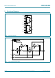

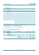
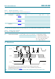
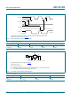
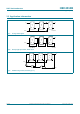

Table Of Contents
- 1. General description
- 2. Features and benefits
- 3. Applications
- 4. Ordering information
- 5. Functional diagram
- 6. Pinning information
- 7. Functional description
- 8. Limiting values
- 9. Recommended operating conditions
- 10. Static characteristics
- 11. Dynamic characteristics
- 12. Waveforms
- 13. Application information
- 14. Package outline
- 15. Revision history
- 16. Legal information
- 17. Contact information
- 18. Contents

HEF4013B All information provided in this document is subject to legal disclaimers. © NXP B.V. 2011. All rights reserved.
Product data sheet Rev. 8 — 21 November 2011 7 of 16
NXP Semiconductors
HEF4013B
Dual D-type flip-flop
[1] Typical values of the propagation delays and output transition times can be calculated with the extrapolation formulas. C
L
is given in pF.
12. Waveforms
t
rec
recovery time nSD input;
see Figure 5
5 V +15 5- ns
10 V 15 0 - ns
15 V 15 0 - ns
nCD input;
see Figure 5
5 V 40 25 - ns
10 V 25 10 - ns
15 V 25 10 - ns
f
clk(max)
maximum clock
frequency
see Figure 4 5 V 7 14 - MHz
10 V 14 28 - MHz
15 V 20 40 - MHz
Table 7. Dynamic characteristics
…continued
T
amb
= 25
C; unless otherwise specified. For test circuit see Figure 6.
Symbol Parameter Conditions V
DD
Extrapolation formula Min Typ Max Unit
Table 8. Dynamic power dissipation
V
SS
= 0 V; t
r
= t
f
20 ns; T
amb
= 25
C.
Symbol Parameter V
DD
Typical formula Where
P
D
dynamic power dissipation 5 V P
D
= 850 f
i
+ (f
o
C
L
) V
DD
2
Wf
i
= input frequency in MHz;
f
o
= output frequency in MHz;
C
L
= output load capacitance in pF;
(f
o
C
L
) = sum of the outputs;
V
DD
= supply voltage in V.
10 V P
D
= 3600 f
i
+ (f
o
C
L
) V
DD
2
W
15 V P
D
= 9000 f
i
+ (f
o
C
L
) V
DD
2
W
Set-up and hold times are shown as positive values but may be specified as negative values.
The shaded areas indicate when the input is permitted to change for predictable output performance.
Measurement points are given in Table 9
.
Fig 4. Set-up time, hold time, minimum clock pulse width, propagation delays and transition times
001aah016
0 V
0 V
t
h
t
su
1/f
clk(max)
t
h
t
su
t
f
t
r
t
W
V
M
V
M
V
M
V
I
V
OH
V
OL
V
I
output nQ
input nCP
input nD
t
t
t
t
t
PHL
t
PLH
V
Y
V
X