
Data Sheet
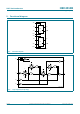

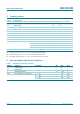
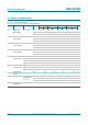
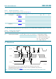
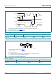

Table Of Contents
- 1. General description
- 2. Features and benefits
- 3. Applications
- 4. Ordering information
- 5. Functional diagram
- 6. Pinning information
- 7. Functional description
- 8. Limiting values
- 9. Recommended operating conditions
- 10. Static characteristics
- 11. Dynamic characteristics
- 12. Waveforms
- 13. Application information
- 14. Package outline
- 15. Revision history
- 16. Legal information
- 17. Contact information
- 18. Contents

HEF4013B All information provided in this document is subject to legal disclaimers. © NXP B.V. 2011. All rights reserved.
Product data sheet Rev. 8 — 21 November 2011 4 of 16
NXP Semiconductors
HEF4013B
Dual D-type flip-flop
8. Limiting values
[1] For DIP14 packages: above T
amb
= 70 C, P
tot
derates linearly with 12 mW/K.
[2] For SO14 packages: above T
amb
= 70 C, P
tot
derates linearly with 8 mW/K.
[3] For TSSOP14 packages: above T
amb
= 60 C, P
tot
derates linearly with 5.5 mW/K.
9. Recommended operating conditions
Table 4. Limiting values
In accordance with the Absolute Maximum Rating System (IEC 60134). Voltages are referenced to V
SS
= 0 V (ground).
Symbol Parameter Conditions Min Max Unit
V
DD
supply voltage 0.5 +18 V
I
IK
input clamping current V
I
< 0.5 V or V
I
>V
DD
+ 0.5 V - 10 mA
V
I
input voltage 0.5 V
DD
+ 0.5 V
I
OK
output clamping current V
O
< 0.5 V or V
O
>V
DD
+ 0.5 V - 10 mA
I
I/O
input/output current - 10 mA
I
DD
supply current - 50 mA
T
stg
storage temperature 65 +150 C
T
amb
ambient temperature 40 +125 C
P
tot
total power dissipation T
amb
= 40 C to +125 C
DIP14
[1]
- 750 mW
SO14
[2]
- 500 mW
TSSOP14
[3]
- 500 mW
P power dissipation per output - 100 mW
Table 5. Recommended operating conditions
Symbol Parameter Conditions Min Max Unit
V
DD
supply voltage 3 15 V
V
I
input voltage 0 V
DD
V
T
amb
ambient temperature 40 +125 C
t/V input transition rise and fall rate V
DD
= 5 V - 3.75 s/V
V
DD
= 10 V - 0.5 s/V
V
DD
= 15 V - 0.08 s/V