
Data Sheet
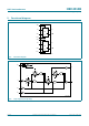

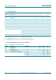
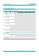
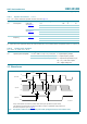
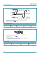
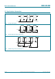

Table Of Contents
- 1. General description
- 2. Features and benefits
- 3. Applications
- 4. Ordering information
- 5. Functional diagram
- 6. Pinning information
- 7. Functional description
- 8. Limiting values
- 9. Recommended operating conditions
- 10. Static characteristics
- 11. Dynamic characteristics
- 12. Waveforms
- 13. Application information
- 14. Package outline
- 15. Revision history
- 16. Legal information
- 17. Contact information
- 18. Contents

HEF4013B All information provided in this document is subject to legal disclaimers. © NXP B.V. 2011. All rights reserved.
Product data sheet Rev. 8 — 21 November 2011 3 of 16
NXP Semiconductors
HEF4013B
Dual D-type flip-flop
6. Pinning information
6.1 Pinning
6.2 Pin description
7. Functional description
[1] H = HIGH voltage level; L = LOW voltage level; X = don’t care; = LOW-to-HIGH clock transition.
Fig 3. Pin configuration
HEF4013B
1Q V
DD
1Q 2Q
1CP 2Q
1CD 2CP
1D 2CD
1SD 2D
V
SS
2SD
001aag085
1
2
3
4
5
6
7 8
10
9
12
11
14
13
Table 2. Pin description
Symbol Pin Description
1Q, 2Q 1, 13 true output
1Q
, 2Q 2, 12 complement output
1CP, 2CP 3, 11 clock input (LOW to HIGH edge-triggered)
1CD, 2CD 4, 10 asynchronous clear-direct input (active HIGH)
1D, 2D 5, 9 data input
1SD, 2SD 6, 8 asynchronous set-direct input (active HIGH)
V
SS
7 ground (0 V)
V
DD
14 supply voltage
Table 3. Function table
[1]
Control Input Output
nSD nCD nCP nD nQ nQ
HLXXHL
LHXXLH
HHXXHH
LL LLH
LL HHL