
Data Sheet
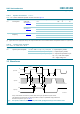
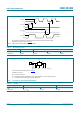

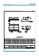
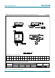
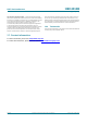
Table Of Contents
- 1. General description
- 2. Features and benefits
- 3. Applications
- 4. Ordering information
- 5. Functional diagram
- 6. Pinning information
- 7. Functional description
- 8. Limiting values
- 9. Recommended operating conditions
- 10. Static characteristics
- 11. Dynamic characteristics
- 12. Waveforms
- 13. Application information
- 14. Package outline
- 15. Revision history
- 16. Legal information
- 17. Contact information
- 18. Contents

HEF4013B All information provided in this document is subject to legal disclaimers. © NXP B.V. 2011. All rights reserved.
Product data sheet Rev. 8 — 21 November 2011 12 of 16
NXP Semiconductors
HEF4013B
Dual D-type flip-flop
Fig 12. Package outline SOT402-1 (TSSOP14)
UNIT A
1
A
2
A
3
b
p
cD
(1)
E
(2) (1)
eH
E
LL
p
QZywv θ
REFERENCES
OUTLINE
VERSION
EUROPEAN
PROJECTION
ISSUE DATE
IEC JEDEC JEITA
mm
0.15
0.05
0.95
0.80
0.30
0.19
0.2
0.1
5.1
4.9
4.5
4.3
0.65
6.6
6.2
0.4
0.3
0.72
0.38
8
0
o
o
0.13 0.10.21
DIMENSIONS (mm are the original dimensions)
Notes
1. Plastic or metal protrusions of 0.15 mm maximum per side are not included.
2. Plastic interlead protrusions of 0.25 mm maximum per side are not included.
0.75
0.50
SOT402-1 MO-153
99-12-27
03-02-18
w M
b
p
D
Z
e
0.25
17
14
8
θ
A
A
1
A
2
L
p
Q
detail X
L
(A )
3
H
E
E
c
v M
A
X
A
y
0 2.5 5 mm
scale
TSSOP14: plastic thin shrink small outline package; 14 leads; body width 4.4 mm
SOT402-1
A
max.
1.1
pin 1 index