
Data Sheet
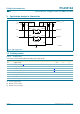

Table Of Contents
- 1. General description
- 2. Features
- 3. Applications
- 4. Feature selection
- 5. Ordering information
- 6. Block diagram
- 7. Pinning information
- 8. Functional description
- 9. Application design-in information
- 10. Limiting values
- 11. Characteristics
- 12. Test information
- 13. Package outline
- 14. Soldering
- 15. Abbreviations
- 16. Revision history
- 17. Data sheet status
- 18. Definitions
- 19. Disclaimers
- 20. Trademarks
- 21. Contact information
- 22. Contents
PCA9512A_1 © Koninklijke Philips Electronics N.V. 2005. All rights reserved.
Product data sheet Rev. 01 — 7 October 2005 13 of 22
Philips Semiconductors
PCA9512A
Level shifting hot swappable I
2
C-bus and SMBus bus buffer
[1] This specification applies over the full operating temperature range.
[2] Card side supply voltage.
[3] The enable time is from power-up of V
CC
and V
CC2
≥ 2.7 V to when idle or stop time begins.
[4] Idle time is from when SDAn and SCLn are HIGH after enable time has been met.
[5] I
trt(pu)
varies with temperature and V
CC
voltage, as shown in Section 11.1 “Typical performance characteristics”.
[6] The connection circuitry always regulates its output to a higher voltage than its input. The magnitude of this offset voltage as a function
of the pull-up resistor and V
CC
voltage is shown in Section 11.1 “Typical performance characteristics”.
[7] Guaranteed by design, not production tested.
[8] C
b
= total capacitance of one bus line in pF.
System characteristics
f
SCL
SCL clock frequency
[7]
0 - 400 kHz
t
BUF
bus free time between
STOP condition and
START condition
[7]
1.3 - - µs
t
HD;STA
START condition hold
time
[7]
0.6 - - µs
t
SU;STA
START condition (or
repeated START
condition) set-up time
[7]
0.6 - - µs
t
SU;STO
STOP condition set-up
time
[7]
0.6 - - µs
t
HD;DAT
data hold time
[7]
300 - - ns
t
SU;DAT
data set-up time
[7]
100 - - ns
t
LOW
SCL LOW time
[7]
1.3 - - µs
t
HIGH
SCL HIGH time
[7]
0.6 - - µs
t
f
fall time SDA and SCL
[7] [8]
20 + 0.1 × C
b
- 300 ns
t
r
rise time SDA and SCL
[7] [8]
20 + 0.1 × C
b
- 300 ns
Table 5: Characteristics
…continued
V
CC
= 2.7 V to 5.5 V; T
amb
=
−
40
°
C to +85
°
C; unless otherwise specified.
Symbol Parameter Conditions Min Typ Max Unit