
Data Sheet
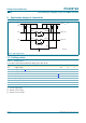
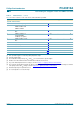

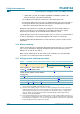
Table Of Contents
- 1. General description
- 2. Features
- 3. Applications
- 4. Feature selection
- 5. Ordering information
- 6. Block diagram
- 7. Pinning information
- 8. Functional description
- 9. Application design-in information
- 10. Limiting values
- 11. Characteristics
- 12. Test information
- 13. Package outline
- 14. Soldering
- 15. Abbreviations
- 16. Revision history
- 17. Data sheet status
- 18. Definitions
- 19. Disclaimers
- 20. Trademarks
- 21. Contact information
- 22. Contents

PCA9512A_1 © Koninklijke Philips Electronics N.V. 2005. All rights reserved.
Product data sheet Rev. 01 — 7 October 2005 12 of 22
Philips Semiconductors
PCA9512A
Level shifting hot swappable I
2
C-bus and SMBus bus buffer
11. Characteristics
Table 5: Characteristics
V
CC
= 2.7 V to 5.5 V; T
amb
=
−
40
°
C to +85
°
C; unless otherwise specified.
Symbol Parameter Conditions Min Typ Max Unit
Power supply
V
CC
supply voltage
[1]
2.7 - 5.5 V
V
CC2
supply voltage 2
[2] [1]
2.7 - 5.5 V
I
CC
supply current V
CC
= 5.5 V;
V
SDAIN
=V
SCLIN
=0V
- 1.8 3.6 mA
I
CC2
supply current 2 V
CC
= 5.5 V;
V
SDAOUT
=V
SCLOUT
=0V
- 1.7 2.9 mA
Start-up circuitry
V
pch
precharge voltage SDA, SCL floating
[1]
0.8 1.1 1.2 V
t
en
enable time on power-up
[3]
- 180 - µs
t
idle
idle time
[1] [4]
50 140 250 µs
Rise time accelerators
I
trt(pu)
transient boosted pull-up
current
positive transition on SDA,
SCL; V
ACC
= 0.7 × V
CC2
;
V
CC
= 2.7 V;
slew rate = 1.25 V/µs
[5]
12-mA
V
th(dis)(ACC)
disable threshold voltage
on pin ACC
0.3V
CC2
0.5V
CC2
-V
V
th(en)(ACC)
enable threshold voltage
on pin ACC
- 0.5V
CC2
0.7V
CC2
V
I
I(ACC)
input current on pin ACC −1 ±0.1 +1 µA
t
PD(on/off)(ACC)
on/off propagation delay
on pin ACC
-5-ns
Input-output connection
V
offset
offset voltage 10 kΩ to V
CC
on SDA, SCL;
V
CC
= 3.3 V; V
CC2
= 3.3 V;
V
I
= 0.2 V
[1] [6]
0 115 175 mV
C
i
input capacitance digital; guaranteed by design,
not subject to test
- - 10 pF
V
OL
LOW-state output voltage V
I
= 0 V; SDAn, SCLn pins;
I
sink
= 3 mA; V
CC
= 2.7 V;
V
CC2
= 2.7 V
[1]
0 0.3 0.4 V
I
LI
input leakage current SDAn, SCLn pins;
V
CC
= 5.5 V; V
CC2
= 5.5 V
−1-+1µA