
Data Sheet
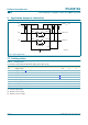
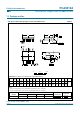

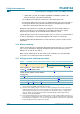
Table Of Contents
- 1. General description
- 2. Features
- 3. Applications
- 4. Feature selection
- 5. Ordering information
- 6. Block diagram
- 7. Pinning information
- 8. Functional description
- 9. Application design-in information
- 10. Limiting values
- 11. Characteristics
- 12. Test information
- 13. Package outline
- 14. Soldering
- 15. Abbreviations
- 16. Revision history
- 17. Data sheet status
- 18. Definitions
- 19. Disclaimers
- 20. Trademarks
- 21. Contact information
- 22. Contents
PCA9512A_1 © Koninklijke Philips Electronics N.V. 2005. All rights reserved.
Product data sheet Rev. 01 — 7 October 2005 11 of 22
Philips Semiconductors
PCA9512A
Level shifting hot swappable I
2
C-bus and SMBus bus buffer
9. Application design-in information
10. Limiting values
[1] Card side supply voltage.
[2] Maximum current for inputs.
[3] Maximum current for I/O pins.
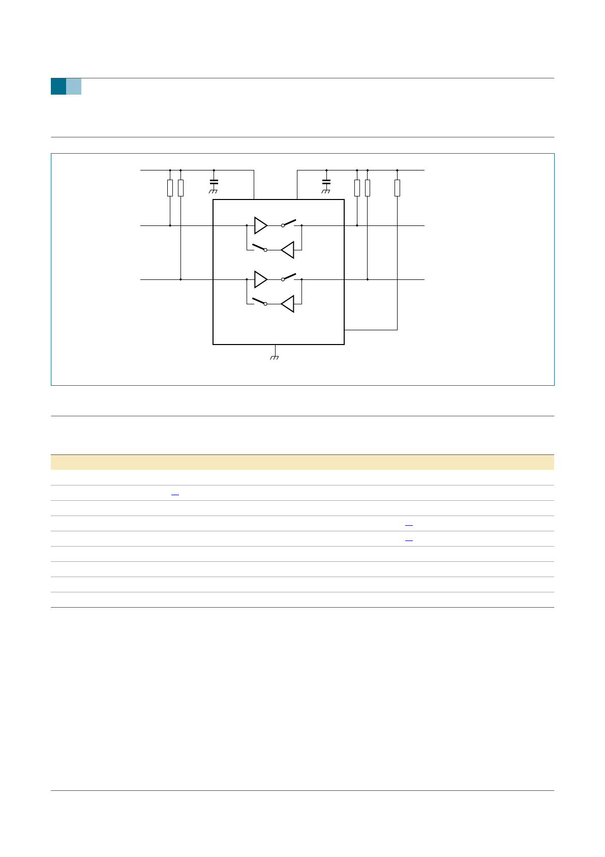
Fig 10. Typical application
002aab794
ACC
GND
R5
10 kΩ
R3
10 kΩ
R4
10 kΩ
SDAOUT
SCLOUT
C2
0.01 µF
R1
10 kΩ
R2
10 kΩ
V
CC
(5 V)
SDAIN
SCLIN
PCA9512A
SDA
SCL
V
CC
V
CC2
C1
0.01 µF
CARD_V
CC
(3 V)
CARD_SDA
CARD_SCL
Table 4: Limiting values
In accordance with the Absolute Maximum Rating System (IEC 60134).
Symbol Parameter Conditions Min Max Unit
V
CC
supply voltage −0.5 +7 V
V
CC2
supply voltage 2
[1]
−0.5 +7 V
V
n
voltage on any other pin −0.5 +7 V
I
I
input current
[2]
- ±20 mA
I
I/O
input/output current
[3]
- ±50 mA
T
oper
operating temperature −40 +85 °C
T
stg
storage temperature −65 +125 °C
T
sp
solder point temperature 10 s maximum - 300 °C
T
j(max)
maximum junction temperature - 125 °C