
Data Sheet

TCS3404, TCS3414
DIGITAL COLOR SENSORS
TAOS137A − APRIL 2011
16
r
r
Copyright E 2011, TAOS Inc.
The LUMENOLOGY r Company
www.taosinc.com
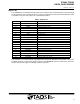
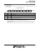
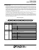
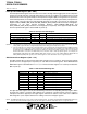
Timing Register (01h)
The TIMING register controls the synchronization and integration time of the ADC channels. The Timing
Register settings apply to all four ADC channels. The Timing Register defaults to 00h at power on.
Table 5. Timing Register
6754
PARAM
2310
0000 0000Reset Value:
TIMING
SYNC_EDGEResv INTEG_MODE01h
FIELD BITS DESCRIPTION
Resv 7 Reserved. Write as 0.
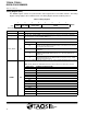
SYNC_EDGE 6
Sync pin edge. If SYNC_EDGE is low, the falling edge of the sync pin is used to stop an integration
cycle when INTEG_MODE is 11. If SYNC_EDGE is high, the rising edge of the sync pin is used to
stop an integration cycle when INTEG_MODE is 11.
Selects preset integration time, manual integration (via serial bus), or external synchronization (SYNC
IN) modes.
FIELD VALUE MODE
00
In this mode, the integrator is free-running and one of the three
internally-generated Nominal Integration Times is selected for each conversion
(see Integration Time table below).
INTEG_MODE 5:4
01
Manually start/stop integration through serial bus using ADC_EN field in Con-
trol Register.
10
Synchronize exactly one internally-timed integration cycle as specified in the
NOMINAL INTEGRATION TIME beginning 2.4 μs after being initiated by the
SYNC IN pin.
11
Integrate over specified number of pulses on SYNC IN pin (See SYNC IN
PULSE COUNT table below). Minimum width of sync pulse is 50 μs. SYNC
IN must be low at least 3.6 μs.
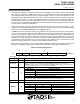
Uses single, multipurpose bitmapped field to select one of three predefined integration times or set the
number of SYNC IN pulses to count when the INTEG_MODE accumulate mode (11) is selected.
NOTE: INTEG_MODE and TIME/COUNTER fields should be written before ADC_EN is asserted.
FIELD VALUE NOMINAL INTEGRATION TIME
0000 12 ms
0001 100 ms
0010 400 ms
PARAM
3:0
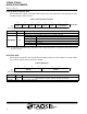
FIELD VALUE SYNC IN PULSE COUNT
PARAM
3
:
0
0000 1
0001 2
0010 4
0011 8
0100 16
0101 32
0110 64
0111 128
1000 256