
Data Sheet

TCS3404, TCS3414
DIGITAL COLOR SENSORS
TAOS137A − APRIL 2011
15
The LUMENOLOGY r Company
r
r
Copyright E 2011, TAOS Inc.
www.taosinc.com
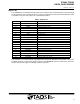
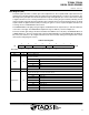
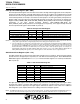
Control Register (00h)
The CONTROL register contains two bits and is primarily used to power the TCS3404/14 device up and down
as shown in Table 4.
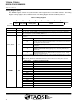
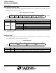
Table 4. Control Register
6754
POWER
2310
0000 0000Reset Value:
CONTROL
ResvResv Resv ADC_VALID Resv
00h
Resv ADC_EN
FIELD BIT DESCRIPTION
Resv 7:6 Reserved. Write as 0.
Resv 5 Reserved. Write as 0.
ADC_VALID 4 ADC valid. This read-only field indicates that the ADC channel has completed an integration cycle.
Resv 3:2 Reserved. Write as 0.
ADC_EN 1
ADC enable. This field enables the four ADC channels to begin integration. Writing a 1 activates the ADC
channels, and writing a 0 disables the ADCs.
POWER 0 Power on. Writing a 1 powers on the device, and writing a 0 turns it off.
NOTES: 1. Both ADC_EN and POWER must be asserted before the ADC channels will operate correctly.
2. INTEG_MODE and TIME/COUNTER fields in the Timing Register (01h) should be written before ADC_EN is asserted.
3. If a value of 03h is written, the value returned during a read cycle will be 03h. This feature can be used to verify that the device is
communicating properly.
4. During writes and reads, the POWER bit is overridden and the oscillator is enabled, independent of the state of POWER.