TCS3404, TCS3414 DIGITAL COLOR SENSORS r r TAOS137A − APRIL 2011 PACKAGE CS 6-LEAD CHIPSCALE (TOP VIEW) Features D Programmable Interrupt Function with User-Defined Upper and Lower Threshold Settings SCL A1 SYNC A2 GND A3 B1 SDA B2 VDD B3 INT D Internal Filter Eliminates Signal Fluctuation Due to AC Lighting Flicker — No External Capacitor Required D In-Package Trim Provides an Easy and Accurate Means to Achieve System-to-System Repeatability D 16-Bit Digital Output with I2C at 400 kHz D Progra
TCS3404, TCS3414 DIGITAL COLOR SENSORS TAOS137A − APRIL 2011 A synchronization input (SYNC) provides precise external control of sensor integration allowing the internal conversion cycles to be synchronized to a pulsed light source. Furthermore, the synchronization feature supports the following advanced modes of operation to maximize flexibility across a broad range of hardware systems: (1) sync for one internal-time cycle, and (2) accumulate for specified number of pulses.
TCS3404, TCS3414 DIGITAL COLOR SENSORS TAOS137A − APRIL 2011 Terminal Functions TERMINAL NAME CS PKG NO. FN PKG NO. TYPE DESCRIPTION GND A3 6 INT B3 4 O Power supply ground. All voltages are referenced to GND. Level interrupt — open drain. SCL A1 1 I Serial clock input terminal — clock signal for I2C serial data. SDA B1 3 I/O SYNC A2 2 I VDD B2 5 Serial data I/O terminal — serial data I/O for I2C. Synchronous input. Supply voltage.
TCS3404, TCS3414 DIGITAL COLOR SENSORS TAOS137A − APRIL 2011 Electrical Characteristics, TA = 25 C (unless otherwise noted) PARAMETER TEST CONDITIONS MIN Power on (ADC inactive) IDD Supply current @ VDD = 3.6 V TYP MAX 7.7 10 UNIT mA Power on (ADC active) 8.7 11 mA Power down 700 1000 μA VOL INT, SDA output low voltage 3 mA sink current I LEAK Input leakage current (SDA, SCL, SYNC) VIH = VDD, VIL = GND 0 0.4 V −5 5 μA AC Electrical Characteristics, VDD = 3.
TCS3404, TCS3414 DIGITAL COLOR SENSORS TAOS137A − APRIL 2011 Optical Characteristics, VDD = 3 V, TA = 25 C, GAIN = 64 , Tint = 12ms (unless otherwise noted) (see Notes 1 and 2) PARAMETER Re Re Irradiance responsivity (CS package) Irradiance responsivity (FN package) TEST CONDITIONS Red Channel MIN TYP Green Channel MAX MIN TYP Blue Channel MAX MIN TYP Clear Channel MAX MIN TYP MAX λp = 470 nm, See Note 3 0% 15% 15% 50% 65% 90% 59.0 65.6 72.
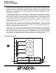
TCS3404, TCS3414 DIGITAL COLOR SENSORS TAOS137A − APRIL 2011 PARAMETER MEASUREMENT INFORMATION t(LOW) t(R) t(F) VIH SCL VIL t(HDSTA) t(BUF) t(HIGH) t(SUSTA) t(HDDAT) t(SUSTO) t(SUDAT) VIH SDA VIL P S Stop Condition S Start Condition Start P Stop t(LOWSEXT) SCLACK SCLACK t(LOWMEXT) t(LOWMEXT) t(LOWMEXT) SCL SDA Figure 2.
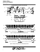
TCS3404, TCS3414 DIGITAL COLOR SENSORS TAOS137A − APRIL 2011 TYPICAL CHARACTERISTICS SPECTRAL RESPONSIVITY CS PACKAGE 120 Clear Clear Red 80 Normalized Responsivity — % Normalized Responsivity — % 100 SPECTRAL RESPONSIVITY FN PACKAGE Green 60 Blue 40 20 100 Red 80 Green 60 Blue 40 20 0 300 400 500 600 700 800 0 300 900 1000 1100 400 500 600 700 800 900 1000 1100 λ − Wavelength − nm λ − Wavelength − nm Figure 5 Figure 6 Note: Spectral responsivity is normalized at 655 nm.
TCS3404, TCS3414 DIGITAL COLOR SENSORS TAOS137A − APRIL 2011 TYPICAL CHARACTERISTICS NORMALIZED RESPONSIVITY vs. ANGULAR DISPLACEMENT — FN PACKAGE NORMALIZED INTEGRATION TIME vs. FREE-AIR TEMPERATURE 106 1.0 105 Normalized Responsivity Tint Normalized — % Internally Timed Integration 103 102 101 100 99 Optical Axis 0.8 104 0.6 0.4 0.
TCS3404, TCS3414 DIGITAL COLOR SENSORS TAOS137A − APRIL 2011 PRINCIPLES OF OPERATION Analog-to-Digital Converter The TCS3404/14 contains four integrating analog-to-digital converters (ADC) that integrate the currents from the four photodiodes (channel 1 through channel 4). Integration of all four channels occurs simultaneously, and upon completion of the conversion cycle the conversion results are transferred to the channel data registers, respectively.
TCS3404, TCS3414 DIGITAL COLOR SENSORS TAOS137A − APRIL 2011 SMBus and I2C Protocols Each Send and Write protocol is, essentially, a series of bytes. A byte sent to the TCS3404/14 with the most significant bit (MSB) equal to 1 will be interpreted as a COMMAND byte. The lower four bits of the COMMAND byte form the register select address (see Table 1), which is used to select the destination for the subsequent byte(s) received.
TCS3404, TCS3414 DIGITAL COLOR SENSORS TAOS137A − APRIL 2011 1 7 1 1 8 1 1 S Slave Address Wr A Data Byte A P X X A Acknowledge (this bit position may be 0 for an ACK or 1 for a NACK) P Stop Condition Rd Read (bit value of 1) S Start Condition Sr Repeated Start Condition Wr Write (bit value of 0) X Shown under a field indicates that that field is required to have a value of X ... Continuation of protocol Master-to-Slave Slave-to-Master Figure 13.
TCS3404, TCS3414 DIGITAL COLOR SENSORS TAOS137A − APRIL 2011 1 7 1 1 8 1 8 1 8 1 1 S Slave Address Wr A Command Code A Data Byte Low A Data Byte High A P Figure 18. SMBus Write Word Protocol 1 S 7 Slave Address 1 1 Wr A 8 Command Code 1 1 7 1 1 8 1 A S Slave Address Rd A Data Byte Low A 8 Data Byte High ... 1 1 A P 1 Figure 19.
TCS3404, TCS3414 DIGITAL COLOR SENSORS TAOS137A − APRIL 2011 Register Set The TCS3404/14 is controlled and monitored by 18 user registers and a command register accessed through the serial interface. These registers provide for a variety of control functions and can be read to determine results of the ADC conversions. The register set is summarized in Table 2. Table 2.
TCS3404, TCS3414 DIGITAL COLOR SENSORS TAOS137A − APRIL 2011 Command Register The command register specifies the address of the target register for subsequent read and write operations. This register contains eight bits as described in Table 3 and defaults to 00h at power on. Table 3. Command Register 7 6 CMD Reset Value: 0 5 BITS CMD 7 3 TRANSACTION 0 FIELD 4 0 2 1 0 COMMAND ADDRESS 0 0 0 0 0 DESCRIPTION Select command register. Must write as 1. Transaction.
TCS3404, TCS3414 DIGITAL COLOR SENSORS TAOS137A − APRIL 2011 Control Register (00h) The CONTROL register contains two bits and is primarily used to power the TCS3404/14 device up and down as shown in Table 4. Table 4. Control Register 7 6 5 4 3 2 1 00h Resv Resv Resv ADC_VALID Resv Resv ADC_EN Reset Value: 0 0 0 0 0 0 0 0 POWER CONTROL 0 FIELD BIT Resv 7:6 Reserved. Write as 0. DESCRIPTION Resv 5 Reserved. Write as 0. ADC_VALID 4 ADC valid.
TCS3404, TCS3414 DIGITAL COLOR SENSORS TAOS137A − APRIL 2011 Timing Register (01h) The TIMING register controls the synchronization and integration time of the ADC channels. The Timing Register settings apply to all four ADC channels. The Timing Register defaults to 00h at power on. Table 5. Timing Register 7 6 01h Resv Reset Value: 0 5 SYNC_EDGE 4 3 2 INTEG_MODE 0 0 0 1 0 TIMING PARAM 0 0 0 0 FIELD BITS Resv 7 Reserved. Write as 0. SYNC_EDGE 6 Sync pin edge.
TCS3404, TCS3414 DIGITAL COLOR SENSORS TAOS137A − APRIL 2011 Interrupt Control Register (02h) The INTERRUPT register controls the extensive interrupt capabilities of the device. The open-drain interrupt pin is active low and requires a pullup resistor to VDD in order to pull high in the inactive state. Using the Interrupt Source Register (03h), the interrupt can be configured to trigger on any one of the four ADC channels.
TCS3404, TCS3414 DIGITAL COLOR SENSORS TAOS137A − APRIL 2011 Interrupt Source Register (03h) The Interrupt Source register selects which ADC channel value to use to generate an interrupt. Only one of the four ADC channels can be selected. Table 7. Interrupt Source Register 7 6 5 4 3 2 03h Resv Resv Resv Resv Resv Resv Reset Value: 0 0 0 0 0 0 FIELD BITS Resv 7:2 1 0 INT SOURCE 0 INT SOURCE 0 DESCRIPTION Reserved. Write as 0. Interrupt Source.
TCS3404, TCS3414 DIGITAL COLOR SENSORS TAOS137A − APRIL 2011 Gain Register (07h) The Gain register provides a common gain control adjustment for all four parallel ADC output channels. Two gain bits [5:4] in the Gain Register allow the relative gain to be adjusted from 1× to 64× in 4× increments. The advantage of the gain adjust is to extend the dynamic range of the light input up to a factor of 64× before analog or digital saturation occurs.
TCS3404, TCS3414 DIGITAL COLOR SENSORS TAOS137A − APRIL 2011 Interrupt Threshold Register (08h − 0Bh) The interrupt threshold registers store the values to be used as the high and low trigger points for the comparison function for interrupt generation. The high and low bytes from each set of registers are combined to form a 16-bit threshold value.
TCS3404, TCS3414 DIGITAL COLOR SENSORS TAOS137A − APRIL 2011 APPLICATION INFORMATION: SOFTWARE Basic Operation After applying VDD, the device will initially be in the power−down state. To operate the device, issue a command to access the control register followed by the data value 03h to the control register to set ADC_EN and POWER to power up the device. At this point, all four ADC channels will begin a conversion at the default integration time of 12 ms.
TCS3404, TCS3414 DIGITAL COLOR SENSORS TAOS137A − APRIL 2011 // Read ADC Channels Using Read Byte Protocol Address = 0x39 Command = 0x90 ReadByte (Address, Command, DataLow) Command = 0x91 ReadByte (Address, Command, DataHigh) Channel1 = 256 * DataHigh + DataLow Command = 0x92 ReadByte (Address, Command, DataLow) Command = 0x93 ReadByte (Address, Command, DataHigh) Channel2 = 256 * DataHigh + DataLow Command = 0x94 ReadByte (Address, Command, DataLow) Command = 0x95 ReadByte (Address, Command, DataHigh) Ch
TCS3404, TCS3414 DIGITAL COLOR SENSORS TAOS137A − APRIL 2011 APPLICATION INFORMATION: SOFTWARE Configuring the Timing Register The command, timing, and control registers are initialized to default values on power up. Setting these registers to the desired values would be part of a normal initialization or setup procedure. In addition, to maximize the performance of the device under various conditions, the integration time and gain may be changed often during operation.
TCS3404, TCS3414 DIGITAL COLOR SENSORS TAOS137A − APRIL 2011 APPLICATION INFORMATION: SOFTWARE Synchronization There are two basic modes of operation for controlling synchronization: (1) internally timed, and (2) externally timed. Internally-timed integration cycles can either be continuous back-to-back conversions or can be externally triggered as a single event using the SYNC pin.
TCS3404, TCS3414 DIGITAL COLOR SENSORS TAOS137A − APRIL 2011 APPLICATION INFORMATION: SOFTWARE When the INTEG_MODE field value is set to 10b, an externally-controlled synchronization input (SYNC) is used to trigger the start of an integration period. The integration period starts on the rising edge of the SYNC pulse, triggers a single, internally-timed integration cycle, and continues until the Nominal Integration Time, as defined in the PARAM field, is completed.
TCS3404, TCS3414 DIGITAL COLOR SENSORS TAOS137A − APRIL 2011 APPLICATION INFORMATION: SOFTWARE When the INTEG_MODE field value is set to 11b, the device integrates from the rising edge of the first pulse until the rising or falling edge of a subsequent pulse as specified by the SYNC_EDGE and PARAM field values. See example timing diagrams below. ADC_EN must be toggled (i.e. from high to low and back to high again) before the next integration cycle.
TCS3404, TCS3414 DIGITAL COLOR SENSORS TAOS137A − APRIL 2011 APPLICATION INFORMATION: SOFTWARE Integration Period SYNC IN INTERRUPT A B NOTE: ADC_EN must be toggled (i.e. from high to low and back to high again) before next integration cycle Figure 25. Integrate Over One Pulse (SYNC_EDGE 0b, INTEG_MODE 11b, PARAM 0b) Falling Edge 1. Enable ADC_EN (= 1) 2. Set SYNC EDGE to 0 3. Set PARAM for SYNC PULSE COUNT of 1 4. Set INTEG_MODE to 11b 5. Input external SYNC pulse 6.
TCS3404, TCS3414 DIGITAL COLOR SENSORS TAOS137A − APRIL 2011 APPLICATION INFORMATION: SOFTWARE Integration Period 1 N SYNC IN INTERRUPT A B NOTE: ADC_EN must be toggled (i.e. from high to low and back to high again) before next integration cycle Figure 27. Integrate Over Two Pulses (SYNC_EDGE 0b, INTEG_MODE 11b, PARAM Xb) Falling Edge 1. Enable ADC_EN (= 1) 2. Set SYNC EDGE to 0 3. Set PARAM for desired SYNC PULSE COUNT 4. Set INTEG_MODE to 11b 5. Input N external SYNC pulse(s) 6.
TCS3404, TCS3414 DIGITAL COLOR SENSORS TAOS137A − APRIL 2011 APPLICATION INFORMATION: SOFTWARE A synchronization input (SYNC IN) is supported to precisely start/stop sensor integration and synchronize with the light source. The TIMING Register (01h) provides two synchronization modes of operation. The first mode of operation synchronizes the SYNC IN pin for one integration cycle as specified in the Timing Register (01h). When the rising edge of the signal is detected, the TCS3404/14 begins integration.
TCS3404, TCS3414 DIGITAL COLOR SENSORS TAOS137A − APRIL 2011 APPLICATION INFORMATION: SOFTWARE Interrupts The interrupt feature of the TCS3404/14 device simplifies and improves system efficiency by eliminating the need to poll the sensor for a light intensity value. Interrupt mode is determined by the INTR field in the Interrupt Control Register. The interrupt feature may be disabled by writing a field value of 00h to the Interrupt Control Register (02h) so that polling can be performed.
TCS3404, TCS3414 DIGITAL COLOR SENSORS TAOS137A − APRIL 2011 APPLICATION INFORMATION: SOFTWARE The following example pseudo code illustrates the configuration of an SMB-Alert style interrupt when the light intensity changes 20% from the current value, and persists for 2.
TCS3404, TCS3414 DIGITAL COLOR SENSORS TAOS137A − APRIL 2011 APPLICATION INFORMATION: HARDWARE Power Supply Decoupling and Application Hardware Circuit The power supply lines must be decoupled with a 0.1 μF capacitor placed as close to the device package as possible (Figure 28).
TCS3404, TCS3414 DIGITAL COLOR SENSORS TAOS137A − APRIL 2011 APPLICATION INFORMATION: HARDWARE PCB Pad Layout for CS Package Suggested PCB pad layout guidelines for the CS package are shown in Figure 29. 0.61 6 0.61 0.30 0.95 NOTES: A. All linear dimensions are in millimeters. B. This drawing is subject to change without notice. Figure 29.
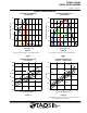
TCS3404, TCS3414 DIGITAL COLOR SENSORS TAOS137A − APRIL 2011 MECHANICAL DATA PACKAGE CS Six-Lead Chipscale TOP VIEW PINOUT TOP VIEW 2095 SCL SYNC GND A1 1565 10 A2 A3 1875 350 10 B1 B2 B3 SDA VDD INT PHOTODIODE ARRAY END VIEW 405 20 685 45 6 160 30 BOTTOM VIEW CL of Photodiode Array Area CL of Solder Bumps 128 Nominal 6 300 30 463 30 CL of Solder Bumps and Photodiode Array Area 950 Nominal Pb 438 30 NOTES: A. B. C. D.
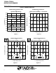
TCS3404, TCS3414 DIGITAL COLOR SENSORS TAOS137A − APRIL 2011 MECHANICAL DATA PACKAGE FN Dual Flat No-Lead TOP VIEW PIN OUT TOP VIEW 350 10 PIN 1 SCL 1 1565 10 3000 100 3000 100 6 GND SYNC 2 5 Vdd SDA 3 4 INT PHOTODIODE ARRAY END VIEW SIDE VIEW 295 Nominal 650 50 203 8 950 BOTTOM VIEW CL of Photodiode Array Area (Note B) 300 50 CL of Solder Contacts 128 Nominal CL of Solder Contacts and Photodiode Array Area (Note B) PIN 1 Pb 950 150 NOTES: A. B. C. D. E. F.
TCS3404, TCS3414 DIGITAL COLOR SENSORS TAOS137A − APRIL 2011 MECHANICAL DATA TOP VIEW 2.00 0.05 1.75 4.00 1.50 4.00 B + 0.30 8.00 − 0.10 3.50 0.05 A B A DETAIL B DETAIL A 5 Max 5 Max 0.254 0.02 2.12 0.05 NOTES: A. B. C. D. E. F. G. 2.30 0.05 1.02 0.05 Ao Bo Ko All linear dimensions are in millimeters. Dimension tolerance is ± 0.10 mm unless otherwise noted. The dimensions on this drawing are for illustrative purposes only.
TCS3404, TCS3414 DIGITAL COLOR SENSORS TAOS137A − APRIL 2011 MECHANICAL DATA TOP VIEW 2.00 0.05 1.75 4.00 1.50 4.00 B + 0.30 8.00 − 0.10 3.50 0.05 A B A DETAIL B DETAIL A 12 Max 10 Max 0.254 0.02 3.30 0.80 3.30 Ao Ko Bo NOTES: H. I. J. K. L. M. N. All linear dimensions are in millimeters. Dimension tolerance is ± 0.10 mm unless otherwise noted. The dimensions on this drawing are for illustrative purposes only. Dimensions of an actual carrier may vary slightly.
TCS3404, TCS3414 DIGITAL COLOR SENSORS TAOS137A − APRIL 2011 MANUFACTURING INFORMATION The CS and FN packages have been tested and has demonstrated an ability to be reflow soldered to a PCB substrate. The solder reflow profile describes the expected maximum heat exposure of components during the solder reflow process of product on a PCB. Temperature is measured on top of component. The components should be limited to a maximum of three passes through this solder reflow profile. Table 12.
TCS3404, TCS3414 DIGITAL COLOR SENSORS TAOS137A − APRIL 2011 MANUFACTURING INFORMATION Moisture Sensitivity Optical characteristics of the device can be adversely affected during the soldering process by the release and vaporization of moisture that has been previously absorbed into the package molding compound. To ensure the package molding compound contains the smallest amount of absorbed moisture possible, each device is dry-baked prior to being packed for shipping.
TCS3404, TCS3414 DIGITAL COLOR SENSORS TAOS137A − APRIL 2011 PRODUCTION DATA — information in this document is current at publication date. Products conform to specifications in accordance with the terms of Texas Advanced Optoelectronic Solutions, Inc. standard warranty. Production processing does not necessarily include testing of all parameters.
Mouser Electronics Authorized Distributor Click to View Pricing, Inventory, Delivery & Lifecycle Information: ams: TCS3404CS TCS3414CS TCS3413CS TCS3404FN TCS3413FN TCS3414FN TCS3415CS TCS3415FN TCS3416CS TCS3416FN