
Data Sheet
Table Of Contents
- Features
- 1. Pin Configurations
- 2. Overview
- 3. Resources
- 4. About Code Examples
- 5. AVR CPU Core
- 6. AVR Memories
- 7. System Clock and Clock Options
- 7.1 Clock Systems and their Distribution
- 7.2 Clock Sources
- 7.3 Low Power Crystal Oscillator
- 7.4 Full Swing Crystal Oscillator
- 7.5 Low Frequency Crystal Oscillator
- 7.6 Calibrated Internal RC Oscillator
- 7.7 128 kHz Internal Oscillator
- 7.8 External Clock
- 7.9 Clock Output Buffer
- 7.10 Timer/Counter Oscillator
- 7.11 System Clock Prescaler
- 7.12 Register Description
- 8. Power Management and Sleep Modes
- 9. System Control and Reset
- 10. Interrupts
- 11. External Interrupts
- 11.1 Pin Change Interrupt Timing
- 11.2 Register Description
- 11.2.1 EICRA - External Interrupt Control Register A
- 11.2.2 EIMSK - External Interrupt Mask Register
- 11.2.3 EIFR - External Interrupt Flag Register
- 11.2.4 PCICR - Pin Change Interrupt Control Register
- 11.2.5 PCIFR - Pin Change Interrupt Flag Register
- 11.2.6 PCMSK2 - Pin Change Mask Register 2
- 11.2.7 PCMSK1 - Pin Change Mask Register 1
- 11.2.8 PCMSK0 - Pin Change Mask Register 0
- 12. I/O-Ports
- 12.1 Overview
- 12.2 Ports as General Digital I/O
- 12.3 Alternate Port Functions
- 12.4 Register Description
- 12.4.1 MCUCR - MCU Control Register
- 12.4.2 PORTB - The Port B Data Register
- 12.4.3 DDRB - The Port B Data Direction Register
- 12.4.4 PINB - The Port B Input Pins Address
- 12.4.5 PORTC - The Port C Data Register
- 12.4.6 DDRC - The Port C Data Direction Register
- 12.4.7 PINC - The Port C Input Pins Address
- 12.4.8 PORTD - The Port D Data Register
- 12.4.9 DDRD - The Port D Data Direction Register
- 12.4.10 PIND - The Port D Input Pins Address
- 13. 8-bit Timer/Counter0 with PWM
- 13.1 Features
- 13.2 Overview
- 13.3 Timer/Counter Clock Sources
- 13.4 Counter Unit
- 13.5 Output Compare Unit
- 13.6 Compare Match Output Unit
- 13.7 Modes of Operation
- 13.8 Timer/Counter Timing Diagrams
- 13.9 Register Description
- 13.9.1 TCCR0A - Timer/Counter Control Register A
- 13.9.2 TCCR0B - Timer/Counter Control Register B
- 13.9.3 TCNT0 - Timer/Counter Register
- 13.9.4 OCR0A - Output Compare Register A
- 13.9.5 OCR0B - Output Compare Register B
- 13.9.6 TIMSK0 - Timer/Counter Interrupt Mask Register
- 13.9.7 TIFR0 - Timer/Counter 0 Interrupt Flag Register
- 14. 16-bit Timer/Counter1 with PWM
- 14.1 Features
- 14.2 Overview
- 14.3 Accessing 16-bit Registers
- 14.4 Timer/Counter Clock Sources
- 14.5 Counter Unit
- 14.6 Input Capture Unit
- 14.7 Output Compare Units
- 14.8 Compare Match Output Unit
- 14.9 Modes of Operation
- 14.10 Timer/Counter Timing Diagrams
- 14.11 Register Description
- 14.11.1 TCCR1A - Timer/Counter1 Control Register A
- 14.11.2 TCCR1B - Timer/Counter1 Control Register B
- 14.11.3 TCCR1C - Timer/Counter1 Control Register C
- 14.11.4 TCNT1H and TCNT1L - Timer/Counter1
- 14.11.5 OCR1AH and OCR1AL - Output Compare Register 1 A
- 14.11.6 OCR1BH and OCR1BL - Output Compare Register 1 B
- 14.11.7 ICR1H and ICR1L - Input Capture Register 1
- 14.11.8 TIMSK1 - Timer/Counter1 Interrupt Mask Register
- 14.11.9 TIFR1 - Timer/Counter1 Interrupt Flag Register
- 15. Timer/Counter0 and Timer/Counter1 Prescalers
- 16. 8-bit Timer/Counter2 with PWM and Asynchronous Operation
- 16.1 Features
- 16.2 Overview
- 16.3 Timer/Counter Clock Sources
- 16.4 Counter Unit
- 16.5 Output Compare Unit
- 16.6 Compare Match Output Unit
- 16.7 Modes of Operation
- 16.8 Timer/Counter Timing Diagrams
- 16.9 Asynchronous Operation of Timer/Counter2
- 16.10 Timer/Counter Prescaler
- 16.11 Register Description
- 16.11.1 TCCR2A - Timer/Counter Control Register A
- 16.11.2 TCCR2B - Timer/Counter Control Register B
- 16.11.3 TCNT2 - Timer/Counter Register
- 16.11.4 OCR2A - Output Compare Register A
- 16.11.5 OCR2B - Output Compare Register B
- 16.11.6 TIMSK2 - Timer/Counter2 Interrupt Mask Register
- 16.11.7 TIFR2 - Timer/Counter2 Interrupt Flag Register
- 16.11.8 ASSR - Asynchronous Status Register
- 16.11.9 GTCCR - General Timer/Counter Control Register
- 17. SPI - Serial Peripheral Interface
- 18. USART0
- 18.1 Features
- 18.2 Overview
- 18.3 Clock Generation
- 18.4 Frame Formats
- 18.5 USART Initialization
- 18.6 Data Transmission - The USART Transmitter
- 18.7 Data Reception - The USART Receiver
- 18.8 Asynchronous Data Reception
- 18.9 Multi-processor Communication Mode
- 18.10 Register Description
- 18.11 Examples of Baud Rate Setting
- 19. USART in SPI Mode
- 20. 2-wire Serial Interface
- 21. Analog Comparator
- 22. Analog-to-Digital Converter
- 23. debugWIRE On-chip Debug System
- 24. Self-Programming the Flash, ATmega48
- 25. Boot Loader Support - Read-While-Write Self-Programming, ATmega88 and ATmega168
- 25.1 Features
- 25.2 Overview
- 25.3 Application and Boot Loader Flash Sections
- 25.4 Read-While-Write and No Read-While-Write Flash Sections
- 25.5 Boot Loader Lock Bits
- 25.6 Entering the Boot Loader Program
- 25.7 Addressing the Flash During Self-Programming
- 25.8 Self-Programming the Flash
- 25.8.1 Performing Page Erase by SPM
- 25.8.2 Filling the Temporary Buffer (Page Loading)
- 25.8.3 Performing a Page Write
- 25.8.4 Using the SPM Interrupt
- 25.8.5 Consideration While Updating BLS
- 25.8.6 Prevent Reading the RWW Section During Self-Programming
- 25.8.7 Setting the Boot Loader Lock Bits by SPM
- 25.8.8 EEPROM Write Prevents Writing to SPMCSR
- 25.8.9 Reading the Fuse and Lock Bits from Software
- 25.8.10 Preventing Flash Corruption
- 25.8.11 Programming Time for Flash when Using SPM
- 25.8.12 Simple Assembly Code Example for a Boot Loader
- 25.8.13 ATmega88 Boot Loader Parameters
- 25.8.14 ATmega168 Boot Loader Parameters
- 25.9 Register Description
- 26. Memory Programming
- 26.1 Program And Data Memory Lock Bits
- 26.2 Fuse Bits
- 26.3 Signature Bytes
- 26.4 Calibration Byte
- 26.5 Page Size
- 26.6 Parallel Programming Parameters, Pin Mapping, and Commands
- 26.7 Parallel Programming
- 26.7.1 Enter Programming Mode
- 26.7.2 Considerations for Efficient Programming
- 26.7.3 Chip Erase
- 26.7.4 Programming the Flash
- 26.7.5 Programming the EEPROM
- 26.7.6 Reading the Flash
- 26.7.7 Reading the EEPROM
- 26.7.8 Programming the Fuse Low Bits
- 26.7.9 Programming the Fuse High Bits
- 26.7.10 Programming the Extended Fuse Bits
- 26.7.11 Programming the Lock Bits
- 26.7.12 Reading the Fuse and Lock Bits
- 26.7.13 Reading the Signature Bytes
- 26.7.14 Reading the Calibration Byte
- 26.7.15 Parallel Programming Characteristics
- 26.8 Serial Downloading
- 27. Electrical Characteristics
- 27.1 Absolute Maximum Ratings*
- 27.2 DC Characteristics ATmega48/88/168*
- 27.3 Speed Grades
- 27.4 Clock Characteristics
- 27.5 System and Reset Characteristics
- 27.6 2-wire Serial Interface Characteristics
- 27.7 SPI Timing Characteristics
- 27.8 ADC Characteristics - Preliminary Data
- 27.9 Parallel Programming Characteristics
- 28. Typical Characteristics - Preliminary Data
- 28.1 Active Supply Current
- 28.2 Idle Supply Current
- 28.3 Supply Current of I/O modules
- 28.4 Power-Down Supply Current
- 28.5 Power-Save Supply Current
- 28.6 Standby Supply Current
- 28.7 Pin Pull-up
- 28.8 Pin Driver Strength
- 28.9 Pin Thresholds and Hysteresis
- 28.10 BOD Thresholds and Analog Comparator Offset
- 28.11 Internal Oscillator Speed
- 28.12 Current Consumption of Peripheral Units
- 28.13 Current Consumption in Reset and Reset Pulse width
- 29. Register Summary
- 30. Instruction Set Summary
- 31. Ordering Information
- 32. Packaging Information
- 33. Errata
- 34. Datasheet Revision History
- Table of Contents
66
2545K–AVR–04/07
ATmega48/88/168
11. External Interrupts
The External Interrupts are triggered by the INT0 and INT1 pins or any of the PCINT23..0 pins.
Observe that, if enabled, the interrupts will trigger even if the INT0 and INT1 or PCINT23..0 pins
are configured as outputs. This feature provides a way of generating a software interrupt. The
pin change interrupt PCI2 will trigger if any enabled PCINT23..16 pin toggles. The pin change
interrupt PCI1 will trigger if any enabled PCINT14..8 pin toggles. The pin change interrupt PCI0
will trigger if any enabled PCINT7..0 pin toggles. The PCMSK2, PCMSK1 and PCMSK0 Regis-
ters control which pins contribute to the pin change interrupts. Pin change interrupts on
PCINT23..0 are detected asynchronously. This implies that these interrupts can be used for
waking the part also from sleep modes other than Idle mode.
The INT0 and INT1 interrupts can be triggered by a falling or rising edge or a low level. This is
set up as indicated in the specification for the External Interrupt Control Register A – EICRA.
When the INT0 or INT1 interrupts are enabled and are configured as level triggered, the inter-
rupts will trigger as long as the pin is held low. Note that recognition of falling or rising edge
interrupts on INT0 or INT1 requires the presence of an I/O clock, described in ”Clock Systems
and their Distribution” on page 27. Low level interrupt on INT0 and INT1 is detected asynchro-
nously. This implies that this interrupt can be used for waking the part also from sleep modes
other than Idle mode. The I/O clock is halted in all sleep modes except Idle mode.
Note that if a level triggered interrupt is used for wake-up from Power-down, the required level
must be held long enough for the MCU to complete the wake-up to trigger the level interrupt. If
the level disappears before the end of the Start-up Time, the MCU will still wake up, but no inter-
rupt will be generated. The start-up time is defined by the SUT and CKSEL Fuses as described
in ”System Clock and Clock Options” on page 27.
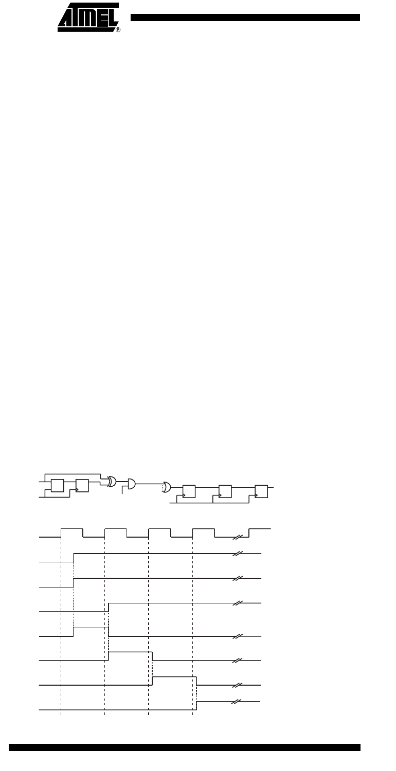
11.1 Pin Change Interrupt Timing
An example of timing of a pin change interrupt is shown in Figure 11-1.
Figure 11-1. Timing of pin change interrupts
clk
PCINT(0)
pin_lat
pin_sync
pcint_in_(0)
pcint_syn
pcint_setflag
PCIF
PCINT(0)
pin_sync
pcint_syn
pin_lat
D Q
LE
pcint_setflag
PCIF
clk
clk
PCINT(0) in PCMSK(x)
pcint_in_(0)
0
x