
Data Sheet
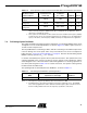

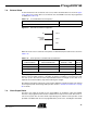
Table Of Contents
- Features
- 1. Pin Configurations
- 2. Overview
- 3. Resources
- 4. About Code Examples
- 5. AVR CPU Core
- 6. AVR Memories
- 7. System Clock and Clock Options
- 7.1 Clock Systems and their Distribution
- 7.2 Clock Sources
- 7.3 Low Power Crystal Oscillator
- 7.4 Full Swing Crystal Oscillator
- 7.5 Low Frequency Crystal Oscillator
- 7.6 Calibrated Internal RC Oscillator
- 7.7 128 kHz Internal Oscillator
- 7.8 External Clock
- 7.9 Clock Output Buffer
- 7.10 Timer/Counter Oscillator
- 7.11 System Clock Prescaler
- 7.12 Register Description
- 8. Power Management and Sleep Modes
- 9. System Control and Reset
- 10. Interrupts
- 11. External Interrupts
- 11.1 Pin Change Interrupt Timing
- 11.2 Register Description
- 11.2.1 EICRA - External Interrupt Control Register A
- 11.2.2 EIMSK - External Interrupt Mask Register
- 11.2.3 EIFR - External Interrupt Flag Register
- 11.2.4 PCICR - Pin Change Interrupt Control Register
- 11.2.5 PCIFR - Pin Change Interrupt Flag Register
- 11.2.6 PCMSK2 - Pin Change Mask Register 2
- 11.2.7 PCMSK1 - Pin Change Mask Register 1
- 11.2.8 PCMSK0 - Pin Change Mask Register 0
- 12. I/O-Ports
- 12.1 Overview
- 12.2 Ports as General Digital I/O
- 12.3 Alternate Port Functions
- 12.4 Register Description
- 12.4.1 MCUCR - MCU Control Register
- 12.4.2 PORTB - The Port B Data Register
- 12.4.3 DDRB - The Port B Data Direction Register
- 12.4.4 PINB - The Port B Input Pins Address
- 12.4.5 PORTC - The Port C Data Register
- 12.4.6 DDRC - The Port C Data Direction Register
- 12.4.7 PINC - The Port C Input Pins Address
- 12.4.8 PORTD - The Port D Data Register
- 12.4.9 DDRD - The Port D Data Direction Register
- 12.4.10 PIND - The Port D Input Pins Address
- 13. 8-bit Timer/Counter0 with PWM
- 13.1 Features
- 13.2 Overview
- 13.3 Timer/Counter Clock Sources
- 13.4 Counter Unit
- 13.5 Output Compare Unit
- 13.6 Compare Match Output Unit
- 13.7 Modes of Operation
- 13.8 Timer/Counter Timing Diagrams
- 13.9 Register Description
- 13.9.1 TCCR0A - Timer/Counter Control Register A
- 13.9.2 TCCR0B - Timer/Counter Control Register B
- 13.9.3 TCNT0 - Timer/Counter Register
- 13.9.4 OCR0A - Output Compare Register A
- 13.9.5 OCR0B - Output Compare Register B
- 13.9.6 TIMSK0 - Timer/Counter Interrupt Mask Register
- 13.9.7 TIFR0 - Timer/Counter 0 Interrupt Flag Register
- 14. 16-bit Timer/Counter1 with PWM
- 14.1 Features
- 14.2 Overview
- 14.3 Accessing 16-bit Registers
- 14.4 Timer/Counter Clock Sources
- 14.5 Counter Unit
- 14.6 Input Capture Unit
- 14.7 Output Compare Units
- 14.8 Compare Match Output Unit
- 14.9 Modes of Operation
- 14.10 Timer/Counter Timing Diagrams
- 14.11 Register Description
- 14.11.1 TCCR1A - Timer/Counter1 Control Register A
- 14.11.2 TCCR1B - Timer/Counter1 Control Register B
- 14.11.3 TCCR1C - Timer/Counter1 Control Register C
- 14.11.4 TCNT1H and TCNT1L - Timer/Counter1
- 14.11.5 OCR1AH and OCR1AL - Output Compare Register 1 A
- 14.11.6 OCR1BH and OCR1BL - Output Compare Register 1 B
- 14.11.7 ICR1H and ICR1L - Input Capture Register 1
- 14.11.8 TIMSK1 - Timer/Counter1 Interrupt Mask Register
- 14.11.9 TIFR1 - Timer/Counter1 Interrupt Flag Register
- 15. Timer/Counter0 and Timer/Counter1 Prescalers
- 16. 8-bit Timer/Counter2 with PWM and Asynchronous Operation
- 16.1 Features
- 16.2 Overview
- 16.3 Timer/Counter Clock Sources
- 16.4 Counter Unit
- 16.5 Output Compare Unit
- 16.6 Compare Match Output Unit
- 16.7 Modes of Operation
- 16.8 Timer/Counter Timing Diagrams
- 16.9 Asynchronous Operation of Timer/Counter2
- 16.10 Timer/Counter Prescaler
- 16.11 Register Description
- 16.11.1 TCCR2A - Timer/Counter Control Register A
- 16.11.2 TCCR2B - Timer/Counter Control Register B
- 16.11.3 TCNT2 - Timer/Counter Register
- 16.11.4 OCR2A - Output Compare Register A
- 16.11.5 OCR2B - Output Compare Register B
- 16.11.6 TIMSK2 - Timer/Counter2 Interrupt Mask Register
- 16.11.7 TIFR2 - Timer/Counter2 Interrupt Flag Register
- 16.11.8 ASSR - Asynchronous Status Register
- 16.11.9 GTCCR - General Timer/Counter Control Register
- 17. SPI - Serial Peripheral Interface
- 18. USART0
- 18.1 Features
- 18.2 Overview
- 18.3 Clock Generation
- 18.4 Frame Formats
- 18.5 USART Initialization
- 18.6 Data Transmission - The USART Transmitter
- 18.7 Data Reception - The USART Receiver
- 18.8 Asynchronous Data Reception
- 18.9 Multi-processor Communication Mode
- 18.10 Register Description
- 18.11 Examples of Baud Rate Setting
- 19. USART in SPI Mode
- 20. 2-wire Serial Interface
- 21. Analog Comparator
- 22. Analog-to-Digital Converter
- 23. debugWIRE On-chip Debug System
- 24. Self-Programming the Flash, ATmega48
- 25. Boot Loader Support - Read-While-Write Self-Programming, ATmega88 and ATmega168
- 25.1 Features
- 25.2 Overview
- 25.3 Application and Boot Loader Flash Sections
- 25.4 Read-While-Write and No Read-While-Write Flash Sections
- 25.5 Boot Loader Lock Bits
- 25.6 Entering the Boot Loader Program
- 25.7 Addressing the Flash During Self-Programming
- 25.8 Self-Programming the Flash
- 25.8.1 Performing Page Erase by SPM
- 25.8.2 Filling the Temporary Buffer (Page Loading)
- 25.8.3 Performing a Page Write
- 25.8.4 Using the SPM Interrupt
- 25.8.5 Consideration While Updating BLS
- 25.8.6 Prevent Reading the RWW Section During Self-Programming
- 25.8.7 Setting the Boot Loader Lock Bits by SPM
- 25.8.8 EEPROM Write Prevents Writing to SPMCSR
- 25.8.9 Reading the Fuse and Lock Bits from Software
- 25.8.10 Preventing Flash Corruption
- 25.8.11 Programming Time for Flash when Using SPM
- 25.8.12 Simple Assembly Code Example for a Boot Loader
- 25.8.13 ATmega88 Boot Loader Parameters
- 25.8.14 ATmega168 Boot Loader Parameters
- 25.9 Register Description
- 26. Memory Programming
- 26.1 Program And Data Memory Lock Bits
- 26.2 Fuse Bits
- 26.3 Signature Bytes
- 26.4 Calibration Byte
- 26.5 Page Size
- 26.6 Parallel Programming Parameters, Pin Mapping, and Commands
- 26.7 Parallel Programming
- 26.7.1 Enter Programming Mode
- 26.7.2 Considerations for Efficient Programming
- 26.7.3 Chip Erase
- 26.7.4 Programming the Flash
- 26.7.5 Programming the EEPROM
- 26.7.6 Reading the Flash
- 26.7.7 Reading the EEPROM
- 26.7.8 Programming the Fuse Low Bits
- 26.7.9 Programming the Fuse High Bits
- 26.7.10 Programming the Extended Fuse Bits
- 26.7.11 Programming the Lock Bits
- 26.7.12 Reading the Fuse and Lock Bits
- 26.7.13 Reading the Signature Bytes
- 26.7.14 Reading the Calibration Byte
- 26.7.15 Parallel Programming Characteristics
- 26.8 Serial Downloading
- 27. Electrical Characteristics
- 27.1 Absolute Maximum Ratings*
- 27.2 DC Characteristics ATmega48/88/168*
- 27.3 Speed Grades
- 27.4 Clock Characteristics
- 27.5 System and Reset Characteristics
- 27.6 2-wire Serial Interface Characteristics
- 27.7 SPI Timing Characteristics
- 27.8 ADC Characteristics - Preliminary Data
- 27.9 Parallel Programming Characteristics
- 28. Typical Characteristics - Preliminary Data
- 28.1 Active Supply Current
- 28.2 Idle Supply Current
- 28.3 Supply Current of I/O modules
- 28.4 Power-Down Supply Current
- 28.5 Power-Save Supply Current
- 28.6 Standby Supply Current
- 28.7 Pin Pull-up
- 28.8 Pin Driver Strength
- 28.9 Pin Thresholds and Hysteresis
- 28.10 BOD Thresholds and Analog Comparator Offset
- 28.11 Internal Oscillator Speed
- 28.12 Current Consumption of Peripheral Units
- 28.13 Current Consumption in Reset and Reset Pulse width
- 29. Register Summary
- 30. Instruction Set Summary
- 31. Ordering Information
- 32. Packaging Information
- 33. Errata
- 34. Datasheet Revision History
- Table of Contents

36
2545K–AVR–04/07
ATmega48/88/168
Oscillator, can be selected when the clock is output on CLKO. If the System Clock Prescaler is
used, it is the divided system clock that is output.
7.10 Timer/Counter Oscillator
The device can operate its Timer/Counter2 from an external 32.768 kHz watch crystal or a exter-
nal clock source. The Timer/Counter Oscillator Pins (TOSC1 and TOSC2) are shared with
XTAL1 and XTAL2. This means that the Timer/Counter Oscillator can only be used when an
internal RC Oscillator is selected as system clock source. See Figure 7-2 on page 30 for crystal
connection.
Applying an external clock source to TOSC1 requires EXTCLK in the ASSR Register written to
logic one. See ”Asynchronous Operation of Timer/Counter2” on page 151 for further description
on selecting external clock as input instead of a 32 kHz crystal.
7.11 System Clock Prescaler
The ATmega48/88/168 has a system clock prescaler, and the system clock can be divided by
setting the ”CLKPR – Clock Prescale Register” on page 377. This feature can be used to
decrease the system clock frequency and the power consumption when the requirement for pro-
cessing power is low. This can be used with all clock source options, and it will affect the clock
frequency of the CPU and all synchronous peripherals. clk
I/O
, clk
ADC
, clk
CPU
, and clk
FLASH
are
divided by a factor as shown in Table 27-3 on page 307.
When switching between prescaler settings, the System Clock Prescaler ensures that no
glitches occurs in the clock system. It also ensures that no intermediate frequency is higher than
neither the clock frequency corresponding to the previous setting, nor the clock frequency corre-
sponding to the new setting. The ripple counter that implements the prescaler runs at the
frequency of the undivided clock, which may be faster than the CPU's clock frequency. Hence, it
is not possible to determine the state of the prescaler - even if it were readable, and the exact
time it takes to switch from one clock division to the other cannot be exactly predicted. From the
time the CLKPS values are written, it takes between T1 + T2 and T1 + 2 * T2 before the new
clock frequency is active. In this interval, 2 active clock edges are produced. Here, T1 is the pre-
vious clock period, and T2 is the period corresponding to the new prescaler setting.
To avoid unintentional changes of clock frequency, a special write procedure must befollowed to
change the CLKPS bits:
1. Write the Clock Prescaler Change Enable (CLKPCE) bit to one and all other bitsin
CLKPR to zero.
2. Within four cycles, write the desired value to CLKPS while writing a zero to CLKPCE.
Interrupts must be disabled when changing prescaler setting to make sure the write procedure is
not interrupted.