
Data Sheet
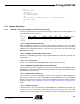
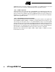
Table Of Contents
- Features
- 1. Pin Configurations
- 2. Overview
- 3. Resources
- 4. About Code Examples
- 5. AVR CPU Core
- 6. AVR Memories
- 7. System Clock and Clock Options
- 7.1 Clock Systems and their Distribution
- 7.2 Clock Sources
- 7.3 Low Power Crystal Oscillator
- 7.4 Full Swing Crystal Oscillator
- 7.5 Low Frequency Crystal Oscillator
- 7.6 Calibrated Internal RC Oscillator
- 7.7 128 kHz Internal Oscillator
- 7.8 External Clock
- 7.9 Clock Output Buffer
- 7.10 Timer/Counter Oscillator
- 7.11 System Clock Prescaler
- 7.12 Register Description
- 8. Power Management and Sleep Modes
- 9. System Control and Reset
- 10. Interrupts
- 11. External Interrupts
- 11.1 Pin Change Interrupt Timing
- 11.2 Register Description
- 11.2.1 EICRA - External Interrupt Control Register A
- 11.2.2 EIMSK - External Interrupt Mask Register
- 11.2.3 EIFR - External Interrupt Flag Register
- 11.2.4 PCICR - Pin Change Interrupt Control Register
- 11.2.5 PCIFR - Pin Change Interrupt Flag Register
- 11.2.6 PCMSK2 - Pin Change Mask Register 2
- 11.2.7 PCMSK1 - Pin Change Mask Register 1
- 11.2.8 PCMSK0 - Pin Change Mask Register 0
- 12. I/O-Ports
- 12.1 Overview
- 12.2 Ports as General Digital I/O
- 12.3 Alternate Port Functions
- 12.4 Register Description
- 12.4.1 MCUCR - MCU Control Register
- 12.4.2 PORTB - The Port B Data Register
- 12.4.3 DDRB - The Port B Data Direction Register
- 12.4.4 PINB - The Port B Input Pins Address
- 12.4.5 PORTC - The Port C Data Register
- 12.4.6 DDRC - The Port C Data Direction Register
- 12.4.7 PINC - The Port C Input Pins Address
- 12.4.8 PORTD - The Port D Data Register
- 12.4.9 DDRD - The Port D Data Direction Register
- 12.4.10 PIND - The Port D Input Pins Address
- 13. 8-bit Timer/Counter0 with PWM
- 13.1 Features
- 13.2 Overview
- 13.3 Timer/Counter Clock Sources
- 13.4 Counter Unit
- 13.5 Output Compare Unit
- 13.6 Compare Match Output Unit
- 13.7 Modes of Operation
- 13.8 Timer/Counter Timing Diagrams
- 13.9 Register Description
- 13.9.1 TCCR0A - Timer/Counter Control Register A
- 13.9.2 TCCR0B - Timer/Counter Control Register B
- 13.9.3 TCNT0 - Timer/Counter Register
- 13.9.4 OCR0A - Output Compare Register A
- 13.9.5 OCR0B - Output Compare Register B
- 13.9.6 TIMSK0 - Timer/Counter Interrupt Mask Register
- 13.9.7 TIFR0 - Timer/Counter 0 Interrupt Flag Register
- 14. 16-bit Timer/Counter1 with PWM
- 14.1 Features
- 14.2 Overview
- 14.3 Accessing 16-bit Registers
- 14.4 Timer/Counter Clock Sources
- 14.5 Counter Unit
- 14.6 Input Capture Unit
- 14.7 Output Compare Units
- 14.8 Compare Match Output Unit
- 14.9 Modes of Operation
- 14.10 Timer/Counter Timing Diagrams
- 14.11 Register Description
- 14.11.1 TCCR1A - Timer/Counter1 Control Register A
- 14.11.2 TCCR1B - Timer/Counter1 Control Register B
- 14.11.3 TCCR1C - Timer/Counter1 Control Register C
- 14.11.4 TCNT1H and TCNT1L - Timer/Counter1
- 14.11.5 OCR1AH and OCR1AL - Output Compare Register 1 A
- 14.11.6 OCR1BH and OCR1BL - Output Compare Register 1 B
- 14.11.7 ICR1H and ICR1L - Input Capture Register 1
- 14.11.8 TIMSK1 - Timer/Counter1 Interrupt Mask Register
- 14.11.9 TIFR1 - Timer/Counter1 Interrupt Flag Register
- 15. Timer/Counter0 and Timer/Counter1 Prescalers
- 16. 8-bit Timer/Counter2 with PWM and Asynchronous Operation
- 16.1 Features
- 16.2 Overview
- 16.3 Timer/Counter Clock Sources
- 16.4 Counter Unit
- 16.5 Output Compare Unit
- 16.6 Compare Match Output Unit
- 16.7 Modes of Operation
- 16.8 Timer/Counter Timing Diagrams
- 16.9 Asynchronous Operation of Timer/Counter2
- 16.10 Timer/Counter Prescaler
- 16.11 Register Description
- 16.11.1 TCCR2A - Timer/Counter Control Register A
- 16.11.2 TCCR2B - Timer/Counter Control Register B
- 16.11.3 TCNT2 - Timer/Counter Register
- 16.11.4 OCR2A - Output Compare Register A
- 16.11.5 OCR2B - Output Compare Register B
- 16.11.6 TIMSK2 - Timer/Counter2 Interrupt Mask Register
- 16.11.7 TIFR2 - Timer/Counter2 Interrupt Flag Register
- 16.11.8 ASSR - Asynchronous Status Register
- 16.11.9 GTCCR - General Timer/Counter Control Register
- 17. SPI - Serial Peripheral Interface
- 18. USART0
- 18.1 Features
- 18.2 Overview
- 18.3 Clock Generation
- 18.4 Frame Formats
- 18.5 USART Initialization
- 18.6 Data Transmission - The USART Transmitter
- 18.7 Data Reception - The USART Receiver
- 18.8 Asynchronous Data Reception
- 18.9 Multi-processor Communication Mode
- 18.10 Register Description
- 18.11 Examples of Baud Rate Setting
- 19. USART in SPI Mode
- 20. 2-wire Serial Interface
- 21. Analog Comparator
- 22. Analog-to-Digital Converter
- 23. debugWIRE On-chip Debug System
- 24. Self-Programming the Flash, ATmega48
- 25. Boot Loader Support - Read-While-Write Self-Programming, ATmega88 and ATmega168
- 25.1 Features
- 25.2 Overview
- 25.3 Application and Boot Loader Flash Sections
- 25.4 Read-While-Write and No Read-While-Write Flash Sections
- 25.5 Boot Loader Lock Bits
- 25.6 Entering the Boot Loader Program
- 25.7 Addressing the Flash During Self-Programming
- 25.8 Self-Programming the Flash
- 25.8.1 Performing Page Erase by SPM
- 25.8.2 Filling the Temporary Buffer (Page Loading)
- 25.8.3 Performing a Page Write
- 25.8.4 Using the SPM Interrupt
- 25.8.5 Consideration While Updating BLS
- 25.8.6 Prevent Reading the RWW Section During Self-Programming
- 25.8.7 Setting the Boot Loader Lock Bits by SPM
- 25.8.8 EEPROM Write Prevents Writing to SPMCSR
- 25.8.9 Reading the Fuse and Lock Bits from Software
- 25.8.10 Preventing Flash Corruption
- 25.8.11 Programming Time for Flash when Using SPM
- 25.8.12 Simple Assembly Code Example for a Boot Loader
- 25.8.13 ATmega88 Boot Loader Parameters
- 25.8.14 ATmega168 Boot Loader Parameters
- 25.9 Register Description
- 26. Memory Programming
- 26.1 Program And Data Memory Lock Bits
- 26.2 Fuse Bits
- 26.3 Signature Bytes
- 26.4 Calibration Byte
- 26.5 Page Size
- 26.6 Parallel Programming Parameters, Pin Mapping, and Commands
- 26.7 Parallel Programming
- 26.7.1 Enter Programming Mode
- 26.7.2 Considerations for Efficient Programming
- 26.7.3 Chip Erase
- 26.7.4 Programming the Flash
- 26.7.5 Programming the EEPROM
- 26.7.6 Reading the Flash
- 26.7.7 Reading the EEPROM
- 26.7.8 Programming the Fuse Low Bits
- 26.7.9 Programming the Fuse High Bits
- 26.7.10 Programming the Extended Fuse Bits
- 26.7.11 Programming the Lock Bits
- 26.7.12 Reading the Fuse and Lock Bits
- 26.7.13 Reading the Signature Bytes
- 26.7.14 Reading the Calibration Byte
- 26.7.15 Parallel Programming Characteristics
- 26.8 Serial Downloading
- 27. Electrical Characteristics
- 27.1 Absolute Maximum Ratings*
- 27.2 DC Characteristics ATmega48/88/168*
- 27.3 Speed Grades
- 27.4 Clock Characteristics
- 27.5 System and Reset Characteristics
- 27.6 2-wire Serial Interface Characteristics
- 27.7 SPI Timing Characteristics
- 27.8 ADC Characteristics - Preliminary Data
- 27.9 Parallel Programming Characteristics
- 28. Typical Characteristics - Preliminary Data
- 28.1 Active Supply Current
- 28.2 Idle Supply Current
- 28.3 Supply Current of I/O modules
- 28.4 Power-Down Supply Current
- 28.5 Power-Save Supply Current
- 28.6 Standby Supply Current
- 28.7 Pin Pull-up
- 28.8 Pin Driver Strength
- 28.9 Pin Thresholds and Hysteresis
- 28.10 BOD Thresholds and Analog Comparator Offset
- 28.11 Internal Oscillator Speed
- 28.12 Current Consumption of Peripheral Units
- 28.13 Current Consumption in Reset and Reset Pulse width
- 29. Register Summary
- 30. Instruction Set Summary
- 31. Ordering Information
- 32. Packaging Information
- 33. Errata
- 34. Datasheet Revision History
- Table of Contents
264
2545K–AVR–04/07
ATmega48/88/168
24.2.1 EEPROM Write Prevents Writing to SPMCSR
Note that an EEPROM write operation will block all software programming to Flash. Reading the
Fuses and Lock bits from software will also be prevented during the EEPROM write operation. It
is recommended that the user checks the status bit (EEPE) in the EECR Register and verifies
that the bit is cleared before writing to the SPMCSR Register.
24.2.2 Reading the Fuse and Lock Bits from Software
It is possible to read both the Fuse and Lock bits from software. To read the Lock bits, load the
Z-pointer with 0x0001 and set the BLBSET and SELFPRGEN bits in SPMCSR. When an LPM
instruction is executed within three CPU cycles after the BLBSET and SELFPRGEN bits are set
in SPMCSR, the value of the Lock bits will be loaded in the destination register. The BLBSET
and SELFPRGEN bits will auto-clear upon completion of reading the Lock bits or if no LPM
instruction is executed within three CPU cycles or no SPM instruction is executed within four
CPU cycles. When BLBSET and SELFPRGEN are cleared, LPM will work as described in the
Instruction set Manual.
The algorithm for reading the Fuse Low byte is similar to the one described above for reading
the Lock bits. To read the Fuse Low byte, load the Z-pointer with 0x0000 and set the BLBSET
and SELFPRGEN bits in SPMCSR. When an LPM instruction is executed within three cycles
after the BLBSET and SELFPRGEN bits are set in the SPMCSR, the value of the Fuse Low byte
(FLB) will be loaded in the destination register as shown below.See Table 26-5 on page 287 for
a detailed description and mapping of the Fuse Low byte.
Similarly, when reading the Fuse High byte (FHB), load 0x0003 in the Z-pointer. When an LPM
instruction is executed within three cycles after the BLBSET and SELFPRGEN bits are set in the
SPMCSR, the value of the Fuse High byte will be loaded in the destination register as shown
below. See Table 26-4 on page 286 for detailed description and mapping of the Extended Fuse
byte.
Similarly, when reading the Extended Fuse byte (EFB), load 0x0002 in the Z-pointer. When an
LPM instruction is executed within three cycles after the BLBSET and SELFPRGEN bits are set
in the SPMCSR, the value of the Extended Fuse byte will be loaded in the destination register as
shown below. See Table 26-5 on page 287 for detailed description and mapping of the Extended
Fuse byte.
Fuse and Lock bits that are programmed, will be read as zero. Fuse and Lock bits that are
unprogrammed, will be read as one.
24.2.3 Preventing Flash Corruption
During periods of low V
CC
, the Flash program can be corrupted because the supply voltage is
too low for the CPU and the Flash to operate properly. These issues are the same as for board
level systems using the Flash, and the same design solutions should be applied.
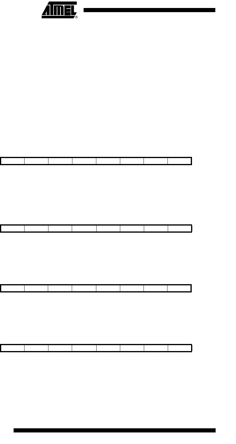
Bit 76543210
Rd ––––––LB2LB1
Bit 76543210
Rd FLB7 FLB6 FLB5 FLB4 FLB3 FLB2 FLB1 FLB0
Bit 76543210
Rd FHB7 FHB6 FHB5 FHB4 FHB3 FHB2 FHB1 FHB0
Bit 76543210
Rd FHB7 FHB6 FHB5 FHB4 FHB3 FHB2 FHB1 FHB0