
Data Sheet
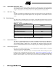

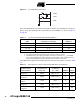
Table Of Contents
- Features
- 1. Pin Configurations
- 2. Overview
- 3. Resources
- 4. About Code Examples
- 5. AVR CPU Core
- 6. AVR Memories
- 7. System Clock and Clock Options
- 7.1 Clock Systems and their Distribution
- 7.2 Clock Sources
- 7.3 Low Power Crystal Oscillator
- 7.4 Full Swing Crystal Oscillator
- 7.5 Low Frequency Crystal Oscillator
- 7.6 Calibrated Internal RC Oscillator
- 7.7 128 kHz Internal Oscillator
- 7.8 External Clock
- 7.9 Clock Output Buffer
- 7.10 Timer/Counter Oscillator
- 7.11 System Clock Prescaler
- 7.12 Register Description
- 8. Power Management and Sleep Modes
- 9. System Control and Reset
- 10. Interrupts
- 11. External Interrupts
- 11.1 Pin Change Interrupt Timing
- 11.2 Register Description
- 11.2.1 EICRA - External Interrupt Control Register A
- 11.2.2 EIMSK - External Interrupt Mask Register
- 11.2.3 EIFR - External Interrupt Flag Register
- 11.2.4 PCICR - Pin Change Interrupt Control Register
- 11.2.5 PCIFR - Pin Change Interrupt Flag Register
- 11.2.6 PCMSK2 - Pin Change Mask Register 2
- 11.2.7 PCMSK1 - Pin Change Mask Register 1
- 11.2.8 PCMSK0 - Pin Change Mask Register 0
- 12. I/O-Ports
- 12.1 Overview
- 12.2 Ports as General Digital I/O
- 12.3 Alternate Port Functions
- 12.4 Register Description
- 12.4.1 MCUCR - MCU Control Register
- 12.4.2 PORTB - The Port B Data Register
- 12.4.3 DDRB - The Port B Data Direction Register
- 12.4.4 PINB - The Port B Input Pins Address
- 12.4.5 PORTC - The Port C Data Register
- 12.4.6 DDRC - The Port C Data Direction Register
- 12.4.7 PINC - The Port C Input Pins Address
- 12.4.8 PORTD - The Port D Data Register
- 12.4.9 DDRD - The Port D Data Direction Register
- 12.4.10 PIND - The Port D Input Pins Address
- 13. 8-bit Timer/Counter0 with PWM
- 13.1 Features
- 13.2 Overview
- 13.3 Timer/Counter Clock Sources
- 13.4 Counter Unit
- 13.5 Output Compare Unit
- 13.6 Compare Match Output Unit
- 13.7 Modes of Operation
- 13.8 Timer/Counter Timing Diagrams
- 13.9 Register Description
- 13.9.1 TCCR0A - Timer/Counter Control Register A
- 13.9.2 TCCR0B - Timer/Counter Control Register B
- 13.9.3 TCNT0 - Timer/Counter Register
- 13.9.4 OCR0A - Output Compare Register A
- 13.9.5 OCR0B - Output Compare Register B
- 13.9.6 TIMSK0 - Timer/Counter Interrupt Mask Register
- 13.9.7 TIFR0 - Timer/Counter 0 Interrupt Flag Register
- 14. 16-bit Timer/Counter1 with PWM
- 14.1 Features
- 14.2 Overview
- 14.3 Accessing 16-bit Registers
- 14.4 Timer/Counter Clock Sources
- 14.5 Counter Unit
- 14.6 Input Capture Unit
- 14.7 Output Compare Units
- 14.8 Compare Match Output Unit
- 14.9 Modes of Operation
- 14.10 Timer/Counter Timing Diagrams
- 14.11 Register Description
- 14.11.1 TCCR1A - Timer/Counter1 Control Register A
- 14.11.2 TCCR1B - Timer/Counter1 Control Register B
- 14.11.3 TCCR1C - Timer/Counter1 Control Register C
- 14.11.4 TCNT1H and TCNT1L - Timer/Counter1
- 14.11.5 OCR1AH and OCR1AL - Output Compare Register 1 A
- 14.11.6 OCR1BH and OCR1BL - Output Compare Register 1 B
- 14.11.7 ICR1H and ICR1L - Input Capture Register 1
- 14.11.8 TIMSK1 - Timer/Counter1 Interrupt Mask Register
- 14.11.9 TIFR1 - Timer/Counter1 Interrupt Flag Register
- 15. Timer/Counter0 and Timer/Counter1 Prescalers
- 16. 8-bit Timer/Counter2 with PWM and Asynchronous Operation
- 16.1 Features
- 16.2 Overview
- 16.3 Timer/Counter Clock Sources
- 16.4 Counter Unit
- 16.5 Output Compare Unit
- 16.6 Compare Match Output Unit
- 16.7 Modes of Operation
- 16.8 Timer/Counter Timing Diagrams
- 16.9 Asynchronous Operation of Timer/Counter2
- 16.10 Timer/Counter Prescaler
- 16.11 Register Description
- 16.11.1 TCCR2A - Timer/Counter Control Register A
- 16.11.2 TCCR2B - Timer/Counter Control Register B
- 16.11.3 TCNT2 - Timer/Counter Register
- 16.11.4 OCR2A - Output Compare Register A
- 16.11.5 OCR2B - Output Compare Register B
- 16.11.6 TIMSK2 - Timer/Counter2 Interrupt Mask Register
- 16.11.7 TIFR2 - Timer/Counter2 Interrupt Flag Register
- 16.11.8 ASSR - Asynchronous Status Register
- 16.11.9 GTCCR - General Timer/Counter Control Register
- 17. SPI - Serial Peripheral Interface
- 18. USART0
- 18.1 Features
- 18.2 Overview
- 18.3 Clock Generation
- 18.4 Frame Formats
- 18.5 USART Initialization
- 18.6 Data Transmission - The USART Transmitter
- 18.7 Data Reception - The USART Receiver
- 18.8 Asynchronous Data Reception
- 18.9 Multi-processor Communication Mode
- 18.10 Register Description
- 18.11 Examples of Baud Rate Setting
- 19. USART in SPI Mode
- 20. 2-wire Serial Interface
- 21. Analog Comparator
- 22. Analog-to-Digital Converter
- 23. debugWIRE On-chip Debug System
- 24. Self-Programming the Flash, ATmega48
- 25. Boot Loader Support - Read-While-Write Self-Programming, ATmega88 and ATmega168
- 25.1 Features
- 25.2 Overview
- 25.3 Application and Boot Loader Flash Sections
- 25.4 Read-While-Write and No Read-While-Write Flash Sections
- 25.5 Boot Loader Lock Bits
- 25.6 Entering the Boot Loader Program
- 25.7 Addressing the Flash During Self-Programming
- 25.8 Self-Programming the Flash
- 25.8.1 Performing Page Erase by SPM
- 25.8.2 Filling the Temporary Buffer (Page Loading)
- 25.8.3 Performing a Page Write
- 25.8.4 Using the SPM Interrupt
- 25.8.5 Consideration While Updating BLS
- 25.8.6 Prevent Reading the RWW Section During Self-Programming
- 25.8.7 Setting the Boot Loader Lock Bits by SPM
- 25.8.8 EEPROM Write Prevents Writing to SPMCSR
- 25.8.9 Reading the Fuse and Lock Bits from Software
- 25.8.10 Preventing Flash Corruption
- 25.8.11 Programming Time for Flash when Using SPM
- 25.8.12 Simple Assembly Code Example for a Boot Loader
- 25.8.13 ATmega88 Boot Loader Parameters
- 25.8.14 ATmega168 Boot Loader Parameters
- 25.9 Register Description
- 26. Memory Programming
- 26.1 Program And Data Memory Lock Bits
- 26.2 Fuse Bits
- 26.3 Signature Bytes
- 26.4 Calibration Byte
- 26.5 Page Size
- 26.6 Parallel Programming Parameters, Pin Mapping, and Commands
- 26.7 Parallel Programming
- 26.7.1 Enter Programming Mode
- 26.7.2 Considerations for Efficient Programming
- 26.7.3 Chip Erase
- 26.7.4 Programming the Flash
- 26.7.5 Programming the EEPROM
- 26.7.6 Reading the Flash
- 26.7.7 Reading the EEPROM
- 26.7.8 Programming the Fuse Low Bits
- 26.7.9 Programming the Fuse High Bits
- 26.7.10 Programming the Extended Fuse Bits
- 26.7.11 Programming the Lock Bits
- 26.7.12 Reading the Fuse and Lock Bits
- 26.7.13 Reading the Signature Bytes
- 26.7.14 Reading the Calibration Byte
- 26.7.15 Parallel Programming Characteristics
- 26.8 Serial Downloading
- 27. Electrical Characteristics
- 27.1 Absolute Maximum Ratings*
- 27.2 DC Characteristics ATmega48/88/168*
- 27.3 Speed Grades
- 27.4 Clock Characteristics
- 27.5 System and Reset Characteristics
- 27.6 2-wire Serial Interface Characteristics
- 27.7 SPI Timing Characteristics
- 27.8 ADC Characteristics - Preliminary Data
- 27.9 Parallel Programming Characteristics
- 28. Typical Characteristics - Preliminary Data
- 28.1 Active Supply Current
- 28.2 Idle Supply Current
- 28.3 Supply Current of I/O modules
- 28.4 Power-Down Supply Current
- 28.5 Power-Save Supply Current
- 28.6 Standby Supply Current
- 28.7 Pin Pull-up
- 28.8 Pin Driver Strength
- 28.9 Pin Thresholds and Hysteresis
- 28.10 BOD Thresholds and Analog Comparator Offset
- 28.11 Internal Oscillator Speed
- 28.12 Current Consumption of Peripheral Units
- 28.13 Current Consumption in Reset and Reset Pulse width
- 29. Register Summary
- 30. Instruction Set Summary
- 31. Ordering Information
- 32. Packaging Information
- 33. Errata
- 34. Datasheet Revision History
- Table of Contents
23
2545K–AVR–04/07
ATmega48/88/168
is set, any write to EEPMn will be ignored. During reset, the EEPMn bits will be reset to 0b00
unless the EEPROM is busy programming.
• Bit 3 – EERIE: EEPROM Ready Interrupt Enable
Writing EERIE to one enables the EEPROM Ready Interrupt if the I bit in SREG is set. Writing
EERIE to zero disables the interrupt. The EEPROM Ready interrupt generates a constant inter-
rupt when EEPE is cleared. The interrupt will not be generated during EEPROM write or SPM.
• Bit 2 – EEMPE: EEPROM Master Write Enable
The EEMPE bit determines whether setting EEPE to one causes the EEPROM to be written.
When EEMPE is set, setting EEPE within four clock cycles will write data to the EEPROM at the
selected address If EEMPE is zero, setting EEPE will have no effect. When EEMPE has been
written to one by software, hardware clears the bit to zero after four clock cycles. See the
description of the EEPE bit for an EEPROM write procedure.
• Bit 1 – EEPE: EEPROM Write Enable
The EEPROM Write Enable Signal EEPE is the write strobe to the EEPROM. When address
and data are correctly set up, the EEPE bit must be written to one to write the value into the
EEPROM. The EEMPE bit must be written to one before a logical one is written to EEPE, other-
wise no EEPROM write takes place. The following procedure should be followed when writing
the EEPROM (the order of steps 3 and 4 is not essential):
1. Wait until EEPE becomes zero.
2. Wait until SELFPRGEN in SPMCSR becomes zero.
3. Write new EEPROM address to EEAR (optional).
4. Write new EEPROM data to EEDR (optional).
5. Write a logical one to the EEMPE bit while writing a zero to EEPE in EECR.
6. Within four clock cycles after setting EEMPE, write a logical one to EEPE.
The EEPROM can not be programmed during a CPU write to the Flash memory. The software
must check that the Flash programming is completed before initiating a new EEPROM write.
Step 2 is only relevant if the software contains a Boot Loader allowing the CPU to program the
Flash. If the Flash is never being updated by the CPU, step 2 can be omitted. See ”Boot Loader
Support – Read-While-Write Self-Programming, ATmega88 and ATmega168” on page 269 for
details about Boot programming.
Caution: An interrupt between step 5 and step 6 will make the write cycle fail, since the
EEPROM Master Write Enable will time-out. If an interrupt routine accessing the EEPROM is
interrupting another EEPROM access, the EEAR or EEDR Register will be modified, causing the
interrupted EEPROM access to fail. It is recommended to have the Global Interrupt Flag cleared
during all the steps to avoid these problems.
Table 6-1. EEPROM Mode Bits
EEPM1 EEPM0
Programming
Time Operation
0 0 3.4 ms Erase and Write in one operation (Atomic Operation)
0 1 1.8 ms Erase Only
1 0 1.8 ms Write Only
1 1 – Reserved for future use