
Data Sheet
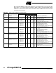
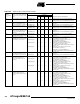
Table Of Contents
- Features
- 1. Pin Configurations
- 2. Overview
- 3. Resources
- 4. About Code Examples
- 5. AVR CPU Core
- 6. AVR Memories
- 7. System Clock and Clock Options
- 7.1 Clock Systems and their Distribution
- 7.2 Clock Sources
- 7.3 Low Power Crystal Oscillator
- 7.4 Full Swing Crystal Oscillator
- 7.5 Low Frequency Crystal Oscillator
- 7.6 Calibrated Internal RC Oscillator
- 7.7 128 kHz Internal Oscillator
- 7.8 External Clock
- 7.9 Clock Output Buffer
- 7.10 Timer/Counter Oscillator
- 7.11 System Clock Prescaler
- 7.12 Register Description
- 8. Power Management and Sleep Modes
- 9. System Control and Reset
- 10. Interrupts
- 11. External Interrupts
- 11.1 Pin Change Interrupt Timing
- 11.2 Register Description
- 11.2.1 EICRA - External Interrupt Control Register A
- 11.2.2 EIMSK - External Interrupt Mask Register
- 11.2.3 EIFR - External Interrupt Flag Register
- 11.2.4 PCICR - Pin Change Interrupt Control Register
- 11.2.5 PCIFR - Pin Change Interrupt Flag Register
- 11.2.6 PCMSK2 - Pin Change Mask Register 2
- 11.2.7 PCMSK1 - Pin Change Mask Register 1
- 11.2.8 PCMSK0 - Pin Change Mask Register 0
- 12. I/O-Ports
- 12.1 Overview
- 12.2 Ports as General Digital I/O
- 12.3 Alternate Port Functions
- 12.4 Register Description
- 12.4.1 MCUCR - MCU Control Register
- 12.4.2 PORTB - The Port B Data Register
- 12.4.3 DDRB - The Port B Data Direction Register
- 12.4.4 PINB - The Port B Input Pins Address
- 12.4.5 PORTC - The Port C Data Register
- 12.4.6 DDRC - The Port C Data Direction Register
- 12.4.7 PINC - The Port C Input Pins Address
- 12.4.8 PORTD - The Port D Data Register
- 12.4.9 DDRD - The Port D Data Direction Register
- 12.4.10 PIND - The Port D Input Pins Address
- 13. 8-bit Timer/Counter0 with PWM
- 13.1 Features
- 13.2 Overview
- 13.3 Timer/Counter Clock Sources
- 13.4 Counter Unit
- 13.5 Output Compare Unit
- 13.6 Compare Match Output Unit
- 13.7 Modes of Operation
- 13.8 Timer/Counter Timing Diagrams
- 13.9 Register Description
- 13.9.1 TCCR0A - Timer/Counter Control Register A
- 13.9.2 TCCR0B - Timer/Counter Control Register B
- 13.9.3 TCNT0 - Timer/Counter Register
- 13.9.4 OCR0A - Output Compare Register A
- 13.9.5 OCR0B - Output Compare Register B
- 13.9.6 TIMSK0 - Timer/Counter Interrupt Mask Register
- 13.9.7 TIFR0 - Timer/Counter 0 Interrupt Flag Register
- 14. 16-bit Timer/Counter1 with PWM
- 14.1 Features
- 14.2 Overview
- 14.3 Accessing 16-bit Registers
- 14.4 Timer/Counter Clock Sources
- 14.5 Counter Unit
- 14.6 Input Capture Unit
- 14.7 Output Compare Units
- 14.8 Compare Match Output Unit
- 14.9 Modes of Operation
- 14.10 Timer/Counter Timing Diagrams
- 14.11 Register Description
- 14.11.1 TCCR1A - Timer/Counter1 Control Register A
- 14.11.2 TCCR1B - Timer/Counter1 Control Register B
- 14.11.3 TCCR1C - Timer/Counter1 Control Register C
- 14.11.4 TCNT1H and TCNT1L - Timer/Counter1
- 14.11.5 OCR1AH and OCR1AL - Output Compare Register 1 A
- 14.11.6 OCR1BH and OCR1BL - Output Compare Register 1 B
- 14.11.7 ICR1H and ICR1L - Input Capture Register 1
- 14.11.8 TIMSK1 - Timer/Counter1 Interrupt Mask Register
- 14.11.9 TIFR1 - Timer/Counter1 Interrupt Flag Register
- 15. Timer/Counter0 and Timer/Counter1 Prescalers
- 16. 8-bit Timer/Counter2 with PWM and Asynchronous Operation
- 16.1 Features
- 16.2 Overview
- 16.3 Timer/Counter Clock Sources
- 16.4 Counter Unit
- 16.5 Output Compare Unit
- 16.6 Compare Match Output Unit
- 16.7 Modes of Operation
- 16.8 Timer/Counter Timing Diagrams
- 16.9 Asynchronous Operation of Timer/Counter2
- 16.10 Timer/Counter Prescaler
- 16.11 Register Description
- 16.11.1 TCCR2A - Timer/Counter Control Register A
- 16.11.2 TCCR2B - Timer/Counter Control Register B
- 16.11.3 TCNT2 - Timer/Counter Register
- 16.11.4 OCR2A - Output Compare Register A
- 16.11.5 OCR2B - Output Compare Register B
- 16.11.6 TIMSK2 - Timer/Counter2 Interrupt Mask Register
- 16.11.7 TIFR2 - Timer/Counter2 Interrupt Flag Register
- 16.11.8 ASSR - Asynchronous Status Register
- 16.11.9 GTCCR - General Timer/Counter Control Register
- 17. SPI - Serial Peripheral Interface
- 18. USART0
- 18.1 Features
- 18.2 Overview
- 18.3 Clock Generation
- 18.4 Frame Formats
- 18.5 USART Initialization
- 18.6 Data Transmission - The USART Transmitter
- 18.7 Data Reception - The USART Receiver
- 18.8 Asynchronous Data Reception
- 18.9 Multi-processor Communication Mode
- 18.10 Register Description
- 18.11 Examples of Baud Rate Setting
- 19. USART in SPI Mode
- 20. 2-wire Serial Interface
- 21. Analog Comparator
- 22. Analog-to-Digital Converter
- 23. debugWIRE On-chip Debug System
- 24. Self-Programming the Flash, ATmega48
- 25. Boot Loader Support - Read-While-Write Self-Programming, ATmega88 and ATmega168
- 25.1 Features
- 25.2 Overview
- 25.3 Application and Boot Loader Flash Sections
- 25.4 Read-While-Write and No Read-While-Write Flash Sections
- 25.5 Boot Loader Lock Bits
- 25.6 Entering the Boot Loader Program
- 25.7 Addressing the Flash During Self-Programming
- 25.8 Self-Programming the Flash
- 25.8.1 Performing Page Erase by SPM
- 25.8.2 Filling the Temporary Buffer (Page Loading)
- 25.8.3 Performing a Page Write
- 25.8.4 Using the SPM Interrupt
- 25.8.5 Consideration While Updating BLS
- 25.8.6 Prevent Reading the RWW Section During Self-Programming
- 25.8.7 Setting the Boot Loader Lock Bits by SPM
- 25.8.8 EEPROM Write Prevents Writing to SPMCSR
- 25.8.9 Reading the Fuse and Lock Bits from Software
- 25.8.10 Preventing Flash Corruption
- 25.8.11 Programming Time for Flash when Using SPM
- 25.8.12 Simple Assembly Code Example for a Boot Loader
- 25.8.13 ATmega88 Boot Loader Parameters
- 25.8.14 ATmega168 Boot Loader Parameters
- 25.9 Register Description
- 26. Memory Programming
- 26.1 Program And Data Memory Lock Bits
- 26.2 Fuse Bits
- 26.3 Signature Bytes
- 26.4 Calibration Byte
- 26.5 Page Size
- 26.6 Parallel Programming Parameters, Pin Mapping, and Commands
- 26.7 Parallel Programming
- 26.7.1 Enter Programming Mode
- 26.7.2 Considerations for Efficient Programming
- 26.7.3 Chip Erase
- 26.7.4 Programming the Flash
- 26.7.5 Programming the EEPROM
- 26.7.6 Reading the Flash
- 26.7.7 Reading the EEPROM
- 26.7.8 Programming the Fuse Low Bits
- 26.7.9 Programming the Fuse High Bits
- 26.7.10 Programming the Extended Fuse Bits
- 26.7.11 Programming the Lock Bits
- 26.7.12 Reading the Fuse and Lock Bits
- 26.7.13 Reading the Signature Bytes
- 26.7.14 Reading the Calibration Byte
- 26.7.15 Parallel Programming Characteristics
- 26.8 Serial Downloading
- 27. Electrical Characteristics
- 27.1 Absolute Maximum Ratings*
- 27.2 DC Characteristics ATmega48/88/168*
- 27.3 Speed Grades
- 27.4 Clock Characteristics
- 27.5 System and Reset Characteristics
- 27.6 2-wire Serial Interface Characteristics
- 27.7 SPI Timing Characteristics
- 27.8 ADC Characteristics - Preliminary Data
- 27.9 Parallel Programming Characteristics
- 28. Typical Characteristics - Preliminary Data
- 28.1 Active Supply Current
- 28.2 Idle Supply Current
- 28.3 Supply Current of I/O modules
- 28.4 Power-Down Supply Current
- 28.5 Power-Save Supply Current
- 28.6 Standby Supply Current
- 28.7 Pin Pull-up
- 28.8 Pin Driver Strength
- 28.9 Pin Thresholds and Hysteresis
- 28.10 BOD Thresholds and Analog Comparator Offset
- 28.11 Internal Oscillator Speed
- 28.12 Current Consumption of Peripheral Units
- 28.13 Current Consumption in Reset and Reset Pulse width
- 29. Register Summary
- 30. Instruction Set Summary
- 31. Ordering Information
- 32. Packaging Information
- 33. Errata
- 34. Datasheet Revision History
- Table of Contents

224
2545K–AVR–04/07
ATmega48/88/168
After a repeated START condition (state 0x10) the 2-wire Serial Interface can access the same
Slave again, or a new Slave without transmitting a STOP condition. Repeated START enables
the Master to switch between Slaves, Master Transmitter mode and Master Receiver mode with-
out losing control of the bus.
Table 20-2. Status codes for Master Transmitter Mode
Status Code
(TWSR)
Prescaler Bits
are 0
Status of the 2-wire Serial Bus
and 2-wire Serial Interface
Hardware
Application Software Response
Next Action Taken by TWI Hardware
To/from TWDR To TWCR
STA STO TWIN
T
TWE
A
0x08 A START condition has been
transmitted
Load SLA+W 0 0 1 X SLA+W will be transmitted;
ACK or NOT ACK will be received
0x10 A repeated START condition
has been transmitted
Load SLA+W or
Load SLA+R
0
0
0
0
1
1
X
X
SLA+W will be transmitted;
ACK or NOT ACK will be received
SLA+R will be transmitted;
Logic will switch to Master Receiver mode
0x18 SLA+W has been transmitted;
ACK has been received
Load data byte or
No TWDR action or
No TWDR action or
No TWDR action
0
1
0
1
0
0
1
1
1
1
1
1
X
X
X
X
Data byte will be transmitted and ACK or NOT ACK will
be received
Repeated START will be transmitted
STOP condition will be transmitted and
TWSTO Flag will be reset
STOP condition followed by a START condition will be
transmitted and TWSTO Flag will be reset
0x20 SLA+W has been transmitted;
NOT ACK has been received
Load data byte or
No TWDR action or
No TWDR action or
No TWDR action
0
1
0
1
0
0
1
1
1
1
1
1
X
X
X
X
Data byte will be transmitted and ACK or NOT ACK will
be received
Repeated START will be transmitted
STOP condition will be transmitted and
TWSTO Flag will be reset
STOP condition followed by a START condition will be
transmitted and TWSTO Flag will be reset
0x28 Data byte has been transmit-
ted;
ACK has been received
Load data byte or
No TWDR action or
No TWDR action or
No TWDR action
0
1
0
1
0
0
1
1
1
1
1
1
X
X
X
X
Data byte will be transmitted and ACK or NOT ACK will
be received
Repeated START will be transmitted
STOP condition will be transmitted and
TWSTO Flag will be reset
STOP condition followed by a START condition will be
transmitted and TWSTO Flag will be reset
0x30 Data byte has been transmit-
ted;
NOT ACK has been received
Load data byte or
No TWDR action or
No TWDR action or
No TWDR action
0
1
0
1
0
0
1
1
1
1
1
1
X
X
X
X
Data byte will be transmitted and ACK or NOT ACK will
be received
Repeated START will be transmitted
STOP condition will be transmitted and
TWSTO Flag will be reset
STOP condition followed by a START condition will be
transmitted and TWSTO Flag will be reset
0x38 Arbitration lost in SLA+W or
data bytes
No TWDR action or
No TWDR action
0
1
0
0
1
1
X
X
2-wire Serial Bus will be released and not addressed
Slave mode entered
A START condition will be transmitted when the bus
becomes free