
Data Sheet
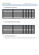

GTI-ATM2022-X-datasheet page 20 of 25
20 / 25
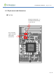
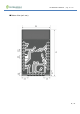
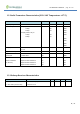
19. Design notes
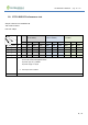
1. Some power rails have to be externally connected, see section-11.
2. The BT RF signal has two routes to the antenna. The 1
st
route goes to the PCB trace antenna through L1, The
2
nd
route goes to pin-2 on the module through the R1 resistor then to the external antenna, the R1 resistor is
not populated as default.
Using the external antenna gives better performance and a longer RF signal range.
Please put on a 0-ohm resistor or 10pF capacitor at the R1 location and remove L1 (see section-8, PCB
placement top view). One SMA antenna socket is recommended in designing the carrier or host board for this
antenna.
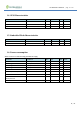
3. The WURX signal on pin-3 is input for Wake up Receiver.
The use of a wake-up receiver allows a system to be in sleep mode while waiting for incoming RF activities. In
the SoC, the wake-up receiver is designed to decode an incoming RF paging or wake-up signal with very low
power consumption. This dedicated low-power wake-up receiver continuously monitors the incoming RF
signal for a predefined paging signal. This continuous Rx mode is based on an OOK radio, which has ultra-
low power consumption. The wake-up receiver is intended for short-range and short-latency applications. The
latency of the wake-up receiver is typically in the order of 20 ms to 1 s, depending on the length of the Rx ID
code used to identify the target device.
In designing the carrier or host board, an SMA antenna socket is recommended going through a serial 10pF
capacitor.