Gleichmann & Co. Electronics GmbH Industriestrasse 16 76297 Stutensee-Spöck / Germany SPECIFICATION CUSTOMER : MODULE NO.: GE- G24064A-TFH-VZ/R APPROVED BY: ( FOR CUSTOMER USE ONLY ) PCB VERSION: SALES BY APPROVED BY DATA: CHECKED BY PREPARED BY ISSUED DATE: VERSION DATE 0 2007-1-31 REVISED SUMMARY PAGE NO.
MODLE NO: DOC. FIRST ISSUE RECORDS OF REVISION VERSION DATE 0 A B 2007-1-31 2007.03.29 2008.11.19 C 2010/1/20 REVISED SUMMARY PAGE NO.
Contents 1. Module Classification Information 2. Precautions in use of LCD Modules 3. General Specification 4. Absolute Maximum Ratings 5. Electrical Characteristics 6. Optical Characteristics 7. Interface Description 8. Contour Drawing & Block Diagram 9. Display Control Instruction 10. Timing Characteristics 11. Reliability 12. Backlight Information 13. Inspection specification 14. Material List of Components for RoHs 15.
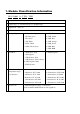
1. Module Classification Information GE-G 24064 A – T F H- VZ/R Brand:Gleichmann Electronics Display Type:C→Character Type, G→Graphic Type Display Font:240 * 64 Model serials no.
2. Precautions in use of LCD Modules (1) Avoid applying excessive shocks to the module or making any alterations or modifications to it. (2) Don’t make extra holes on the printed circuit board, modify its shape or change the components of LCD module. (3) Don’t disassemble the LCM. (4) Don’t operate it above the absolute maximum rating. (5) Don’t drop, bend or twist LCM. (6) Soldering:only to the I/O terminals. (7) Storage:please storage in anti-static electricity container and clean environment. 3.
4.Absolute Maximum Ratings Item Symbol Min Typ Max Unit Operating Temperature TOP -20 - 70 ℃ Storage Temperature TST -30 - +80 ℃ Input Voltage VI Vss - VDD V Supply Voltage VDD-VSS -0.3 - +7 V Supply Voltage For LCD VDD-V0 0 - 15 V Negative Voltage Output VEE - 10 - V 5.Electrical Characteristics Item Supply Voltage For Logic Symbol Condition Min Typ Max Unit VDD-VSS - 4.75 5.0 5.25 V Ta=-20℃ - - 13.9 V Ta=25℃ - 12.5 - V Ta=+70℃ 10.
6.
7.Interface Description Pin No. Symbol Level Description 1 FG - Frame ground ( Connected to bezel ) 2 Vss - GND 3 Vdd - Power supply ( +5 V ) 4 Vo - Power supply for LCD driver 5 WR L Data write. Write data into RA6963 when WR = L 6 RD L Data read.
8.Contour Drawing &Block Diagram 180.0 0.5 2.0 176.0 15.56 23.5 154.6 133.0(V A) 26.42 127.16(AA) 4.13 12.3M ax 7.7 PIN 3 K 2.54 A 2.54 5D -SL001-03 LED B/L RED LINE A K K W HITE LINE DOT SIZE SCA LE 10/1 C om ponent Side H L Rev Nor Rev select VR 10K~20K Vdd,V1,V4,V5 EIO 240X64 DOT NT7086 Seg1~80 Seg Driver NT7086 Seg81~160 Seg Driver Address Data 32K8 SRAM 32K optional Reverse Circuit RV Vdd Vo Vee External contrast adjustment.
9.Display control instruction 9.1 Communications with MPU •Status Read A status check must be performed before data is read or written. Status Check The Status of RA6963 can be read from the data lines. The RA6963 status word format is as follows: Note 1: It is necessary to check STA0 and STA1 at the same time. There is a possibility of erroneous operation due to a hardware interrupt. Note 2: For most modes STA0 /STA1 are used as a status check.
Note 4: When using the MSB=0 command, a Status Read must be performed. If a status check is not carried out, the RA6963 cannot operate normally, even after a delay time. The hardware interrupt occurs during the address calculation period (at the end of each line). If a MSB=0 command is sent to the RA6963 during this period, the RA6963 enters Wait status. If a status check is not carried out in this state before the next command is sent, there is the possibility that command or data will not be received.
• Command Definitions
9.2 Setting Registers • Set Cursor Pointer The X-Adrs and Y-Adrs specify the position of the cursor. The cursor position can only be moved by this command. Data read /write from the MPU never changes the cursor pointer. X-Adrs and Y-Adrs are specified as follows.
• Set Offset Register The offset register is used to determine the external character generator RAM area. The RA6963 has a 16-bit address bus as follows: RA6963 assign External character generator, when character code set 80h to FFh in using Internal character generator. Character code 00h to 80h assign External character generator, when External generator mode The senior five bits define the start address in external memory of the CG RAM area.
• Set Address Pointer The Set Address Pointer command is used to indicate the start address for writing to (or reading from) External RAM.
9.3 Set Control Word The home address and column size are defined by this command. • Set Text Home Address The starting address in the external display RAM for text display is defined by this command. The text home address indicates the leftmost and uppermost position.
• Set Graphic Home Address The starting address of the external display RAM used for graphic display is defined by this Command. The graphic home address indicates the leftmost and uppermost position.
• Set Text Area The display columns are defined by the hardware setting. This command can be used adjust the columns of the display. • Set Graphic Area The display columns are defined by the hardware setting. This command can be used to adjust the columns of the graphic display. If the graphic area setting is set to match the desired number of columns on the LCD, the addressing scheme will be automatically modified so that the start address of each line equals the end address of the previous line +1.
9.4 Mode Set The display mode is defined by this command. The display mode does not change until the next command is sent. The logical OR, EXOR, AND of text or graphic display can be displayed. In internal Character Generator mode, character codes 00h to 7Fh are assigned to the built-in Character generator ROM. The character codes 80h to FFh are automatically assigned to the external character generator RAM.
9.
9.6 Cursor Pattern Select 9.7 Data Auto Read/Write This command is convenient for sending a full screen of data from the external display RAM. After Setting Auto mode, a Data Write (or Read) command does not need sent between each datum. A Data Auto Write (or Read) command must be sent after a Set Address Pointer command. After this Command, the address pointer is automatically incremented by 1 after each datum. In Auto mode, the RA6963 cannot accept any other commands.
9.8 Data Read/Write This command is used for writing data from the MPU to external display RAM, and reading data from external display RAM. Data Write / Data Read should be executed after setting address using Set Address Pointer command, The address pointer can be automatically incremented or decremented using this command. Note: This command is necessary for each 1-byte datum. Refer to the following flowchart.
9.9 Screen Peek This command is used to transfer 1 byte of displayed data to the data stack; this byte can be read from the MPU by data access. The logical combination of text and graphic display data on the LCD screen can be read by this command. The status (STA6) should be checked just after the Screen Peek command. If the address Determined by the Set Address Pointer command is not in the graphic area, this command is ignored and a status flag (STA6) is set. Refer to the following flowchart.
9-10 Screen Copy This command copies a single raster line of data to the graphic area. The start point must be set using the Set Address Pointer command. Note 1: If the attribute function is being used, this command is not available. (With Attribute data is graphic area data.) Note 2: With Dual-Scan, this command cannot be used (because the RA6963 cannot separate the upper screen data and lower screen data). Refer to the following flowchart.
9-11 Bit Set/Reset This command used to set or reset a bit of the byte specified by the address pointer. Only one bit can be set / reset at time. Refer to following flowchart.
9-12 Screen Reverse Bit0 = 0: Normally display. Bit0 = 1: Reverse the whole screen. This command (D0h) is used to reverse the displayed data of the whole screen. When this function is enabled, the displayed data on the LCD are reversed to show reversing pattern. 9-13 Blink Time The blink time of the blink functions are adjusted by this command (50h). For example, if the frequency of the frame equals 60Hz, the blink time can be adjusted from 0.066 second to 2 second by using software selections.
9-14 Cursor Auto Moving Bit0 = 0: Disable. Bit0 = 1: Enable. The RA6963 provides a unique function for the automatic cursor movement. After writing (reading) each displayed datum, the cursor pointer is automatically increased/decreased by one in the Cursor Auto-Moving mode. 9-15 CGROM Font Select This command (70h) is a convenient function for selecting the Character Font Map. The user can get more built-in characters from CGROM Font-01 or CGROM Font-02, which is determined by software selections.
9-16 Character Font Map The RA6963 has two part number - RA6963L2NA and RA6963L2NB. The RA6963L2NA is compatible to T6963C(code 0101) and the default font is Figure 6-13 as above. The RA6963L2NB is compatible to T6963C(code 0201) and the default font is Figure 6-14 as above. Although RA6963 provide a extra internal command for MCU to select both font of above, but you do not need to change the software to select the font that if you chose the right part number.
9-17 RA6963 vs.
10.
Driver Interface Timing (VDD=+5V±5%,GND=0V,Ta= -20 to +70℃)
External Memory Interface (VDD=+5V±5%,GND=0V,Ta= -20 to +70℃)
11. Reliability Content of Reliability Test (wide temperature, -20°C~70°C) Environmental Test Test Item High Temperature storage Low Temperature storage High Temperature Operation Low Temperature Operation High Temperature/ Humidity Operation Thermal shock resistance Content of Test Endurance test applying the high storage temperature for a long time. Endurance test applying the high storage temperature for a long time.
12.Backlight Information Specification PARAMETER SYMBOL MIN Supply Current ILED Supply Voltage Reverse Voltage Luminous Intensity TYP MAX 72 80 V 3.4 VR IV LED Life Time - Color White UNIT TEST 125 mA V=3.5V 3.5 3.6 V - - - 5 V - 180 220 - CD/M2 ILED=80mA - 50K - Hr. CONDITION ILED=80mA 25℃ ℃,50-60%RH, Note 1 Note: The LED of B/L is drive by current only, drive voltage is for reference only.
13. Inspection specification NO 01 02 Item Criterion AQL Electrical Testing 1.1 Missing vertical, horizontal segment, segment contrast defect. 1.2 Missing character , dot or icon. 1.3 Display malfunction. 1.4 No function or no display. 1.5 Current consumption exceeds product specifications. 1.6 LCD viewing angle defect. 1.7 Mixed product types. 1.8 Contrast defect. 0.65 Black or white 2.1 White and black spots on display ≦0.25mm, no more than spots on LCD three white or black spots present.
NO Item 05 Scratches Criterion AQL Follow NO.3 LCD black spots, white spots, contamination Symbols Define: x: Chip length y: Chip width z: Chip thickness k: Seal width t: Glass thickness a: LCD side length L: Electrode pad length: 6.1 General glass chip : 6.1.1 Chip on panel surface and crack between panels: 06 Chipped glass z: Chip thickness y: Chip width x: Chip length Z≦1/2t Not over viewing area x≦1/8a 1/2t<z≦2t Not exceed 1/3k x≦1/8a 2.
NO Item Criterion AQL Symbols : x: Chip length y: Chip width z: Chip thickness k: Seal width t: Glass thickness a: LCD side length L: Electrode pad length 6.2 Protrusion over terminal : 6.2.1 Chip on electrode pad : y: Chip width x: Chip length z: Chip thickness y≦0.5mm x≦1/8a 0<z≦t 6.2.2 Non-conductive portion: 06 Glass crack 2.
NO Item 07 Cracked glass 08 09 10 Backlight elements Bezel PCB、COB Criterion AQL The LCD with extensive crack is not acceptable. 2.5 8.1 Illumination source flickers when lit. 8.2 Spots or scratched that appear when lit must be judged. Using LCD spot, lines and contamination standards. 8.3 Backlight doesn’t light or colour wrong. 0.65 2.5 0.65 9.1 Bezel may not have rust, be deformed or have fingerprints, stains or other contamination. 9.2 Bezel must comply with job specifications. 2.5 0.
NO Item Criterion AQL 12.1 No oxidation, contamination, curves or, bends on interface Pin (OLB) of TCP. 12.2 No cracks on interface pin (OLB) of TCP. 12.3 No contamination, solder residue or solder balls on product. 12.4 The IC on the TCP may not be damaged, circuits. 12.5 The uppermost edge of the protective strip on the interface pin must be present or look as if it cause the interface pin to sever. 12 General appearance 12.
14. Material list of components for RoHS 1. The manufacturer hereby declares that all of or part of products (with the mark “/R” in code), including, but not limited to, the LCM, accessories or packages, manufactured and/or delivered to your company (including your subsidiaries and affiliated company) directly or indirectly by our company (including our subsidiaries or affiliated companies) do not intentionally contain any of the substances listed in EU-Directive 2002/95/EC.