
Datasheet


GE-G12864A-YYH-V/RN page 19 / 22 18.02.2009
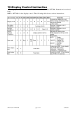
06
Glass
crack
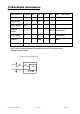
Symbols :
x: Chip length y: Chip width z: Chip thickness
k: Seal width t: Glass thickness a: LCD side length
L: Electrode pad length
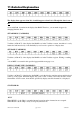
6.2 Protrusion over terminal :
6.2.1 Chip on electrode pad :
y: Chip width x: Chip length z: Chip thickness
y≦0.5mm x≦1/8a 0 < z ≦ t
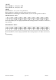
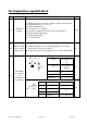
6.2.2 Non-conductive portion:
y: Chip width x: Chip length z: Chip
thickness
y≦ L x≦1/8a 0 < z ≦ t
☉If the chipped area touches the ITO terminal, over 2/3 of the
ITO must remain and be inspected according to electrode
terminal specifications.
☉If the product will be heat sealed by the customer, the
alignment mark not be damaged.
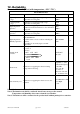
6.2.3 Substrate protuberance and internal crack.
y: width x: length
y≦1/3L x ≦ a
2.5