
User's Manual


apmcomm confidential
apm6658/6659 WiFi 802.11 b/g/n & BT2.1+EDR Dual Radio Module
Product Information Data Sheet
Page 29 of 30
apm Communication, Inc. – TEL: 886-3-666-1188 – FAX: 886-3-666-8033
Website: http://www.apmcomm.com – E-mail:
sales@apmcomm.com
apmcomm Proprietary and Confidential – Product information is subject to change without notice.– May 30 2011
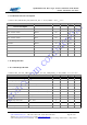
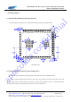
‧ The solder paste pattern for the internal Tab pads could be split into 4 smaller segments for the 2 large pads, and
2 smaller segments for the smaller pads, this should have the effect of preventing the paste from pooling into one area,
and hence minimize the likelihood of the pads being held away from each other. We use a rule of thumb of 50% solder
paste area in relation to Tab copper area (this only applies to tab pads under the device – not the signal pads).
‧ The thickness of the solder paste stencil has implications on solder joint quality as well, we do not have the
knowledge on what stencil should be specified.
‧ Ensure they are using a good appropriate flux, and the correct reflow profile for unleaded (basically +20C above
leaded) which is also uniform in nature.
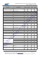
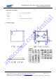
Violating the basic rules might cause problems. For example, if the stencil apertures of the internal ground planes
are improperly big, they would hold more solders in SMT process and may cause the module peripheral pads
un-contacted to the main board. To improve this situation, apmcomm suggests the stencil opening shown as follows.
Stencil Aperture (Top View)