
User's Manual


apmcomm confidential
apm6658/6659 WiFi 802.11 b/g/n & BT2.1+EDR Dual Radio Module
Product Information Data Sheet
Page 28 of 30
apm Communication, Inc. – TEL: 886-3-666-1188 – FAX: 886-3-666-8033
Website: http://www.apmcomm.com – E-mail:
sales@apmcomm.com
apmcomm Proprietary and Confidential – Product information is subject to change without notice.– May 30 2011
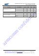
4 Assembly Guideline
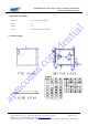
4-1 Recommended Mounting Pad Design (Top View)
The following figure illustrates the recommended mounting pad design for apm6658/6659.
TOP VIEW (mm)
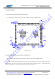
4-2 Recommendation for Stencil Aperture in SMT Process
Please follow general QFN stencil design guideline. Some rules of thumb are highlighted below.
‧ The LGA pads should NOT be flooded over with copper, they should be connected into the plane with a track
width of approx 50% of the pad width, this will mean more heat will be available at the joint. Track lengths should
obviously be minimized, we would generally use about 0.3mm on external layers.