
User's Manual
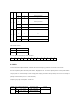

Final TR (Q26) amplify RF Carrier as much as around 15dBm in the finial part of amplification. R96, VR14 and Q33
decide TX Power. Q33 and VR alter SD-5200 from 5W to 2W. When MPU (U13) becomes high, Q33 will be "ON" by
dropping the gate pow er of TR (Q26).
When MPU (U13) P1.0 Port becomes High, Q33 will be ON, and alter power form 5W to 2W by dropping gate power of
final TR(Q26) VR14 will control 2W RF power.
APC is designed to be operated when power is 2W
APC senses RF carrier from Final AMP and low supply power when RF Power is higher more than 2W. When RF Power
is less than 2W, APC increase supply power of power Drive in order to make RF Power maintain 2W.
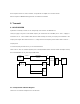
APC (Automatic Power Control) consist of RF Carrier sensor, amplification part that compare with standard voltage and
schematic that switch the checked voltage.
RF Carrier sensor will be changed to DC voltage by using C116, D20, C134 in order to supply base voltage of Q36 in the
amplification part.
The voltage which is supplied to Q36 is arrange low power(2W) with VR14, High Power(5W) control Q33 (when Base is
high).
Q36 in the amplification compare base voltage of Q36 which come from sensor part with base standard voltage which is
supplied to Q36 and control Q35 which control RF pow er to be 2W by controlling base voltage of Q30.
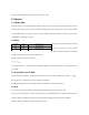
2.6 Antenna Switch
Antenna switch is consist of TX carrier, switching part and low pass filter. Switching part choose RF RX signal and low
pass filter eliminate spurious at TX.
TX and RX switching part is operated by Pin Diode D10, D11.
At TX, when TX+8V provide power to L36, R98 and C113, D10 and D11 turn on, RF carrier flowing receiving direction is
isolated and emit to antenna. At RX, when power providing to Pin diode of TX+8V turn off, D10 and D11 turn off and RF
carrier is provided to receiving direction.